Social Icons

Pages

Temperature warning indicator circuit

The circuit is a low temperature regulator, supervisor, warns us about global warming. Temperature control is done by the thermistor TH1, which is a negative factor. The resistance varies between 10KO at 25 ° C and about 1KO at 94 ° C. The trimmer TR1 regulate the exact temperature at which the Q1-2, connected as a Darlington, lead me, making the relay K1 to close and IZ, sound.


The alarm is activated when the temperature is greater than the default. The thermistor should be located away from the rest of the circuit, so as not to risk from the heat. The power circuit is battery 9V, but if it is mounted in a fixed position, then we can supply with a constant voltage power supply. The relay contacts can be connected load which we, as a bulb, another circuit, etc. It can also add an LED, if we are to sign and visual stimulation.


The adjustment is done by immersing the thermistor TH1, in the water which we know the temperature (contacts should be well insulated so we do not have short circuit) and adjusting the trimmer until the circuit is excited. The cable connecting the circuit with the TH1 must be shielded.

Temperature warning indicator circuit


Temperature warning indicator circuit


Part List
R1= 820 ohm
R2-3= 1Kohm
C1= 220uF 16V
TR1= 2.2Kohm Trimmer D1= 5.6V 0.5W Zener
D2-3= 1N4148
Q1-2= BC550C
TH1= Thermistor 10Kohm at 25° C
K1= 6V 200 ohm Relay
BZ1= Buzzer
S1= 1×2 Switch
BATT= Battery 9V or external supply

Application

 
This circuit is designed not only setting a detection of high temperatures, but can also be changed to be set on the detection of low temperatures in some areas. It can be used for refrigeration, walk-in refrigerator or freezer and other environments that are sensitive to temperature. Some integrated circuits high-temperature alarm modules will be used in motor vehicles to the profession in which the temperature element senses a temperature very dangerous in the interior of a motor vehicle, and encourages the employment sensor detects the presence or determine the absence of an occupant. In the absence of the inhabitants, the sensor is that after a period during which an audible alarm is activated to provide the attention to the motor vehicle in the presence of an occupant. This type of alarm can be reset with a key.
Take a temperature alarm can be advantages such as protection of valuable equipment by high temperature, low temperature, high humidity or sometimes provided. Other programs of high temperature can be used to protect against loss of or against the air conditioning system for heating off. Instead, the program for low-temperature failure of the heating system be used to prevent frozen pipes. The alarm can also reduce downtime, get a phone call and the notification of a possible power failure or failure before damage occurs in one unit

Simplest Transformerless LED Drivers

In this post we learn regarding three interesting transformerless power supply circuits for illuminating LEDs from mains that uses minimum number of components


Circuit 1


Simplest Transformerless LED Drivers


A capacitor must be having a rating of more than 200V and should be having dialectic of metallize polyester or poly poplin.

A resistor 1K is employed to limit the in rush current the resistor should be having the wattage value of more than 1Watt.

A diode is connected in anti-parallel to the LED. This diode limits the reverse voltage across the LED. The diode also provides the path for the negative half cycle as the LED is connected to a AC power source.

This particular circuit behaves like a constant current source of 15 to 20mA depending on LED voltage bias and supply line stability with a nominal 60Hz power supply frequency. The circuit 2 is an improvisation over circuit 1 and it enables to glow two LED’s at a time. This gives a color benefit also.

Putting two switches to the series part of individual LEDs can enable the viewer to have three colors.

In this transformerless circuit using the above formula the current can be manipulated by changing the capacitor value. Power LEDs can also be driven directly from AC power source.

Circuit2


Simplest Transformerless LED Drivers


The third circuit employs a zener diode of 5.6 V/1W. The zener diode serves dual purpose. Firstly it acts as a bias of the negative half of circuit like the diodes employed in circuit 1 and 2. Secondly, it acts as a voltage regulator for the LED driver circuit.

This circuit provides 5 Volts steady output with a 30mA current pumping facility. The 1000uF capacitor acts as a ripple suppressor and it allows a moderate ripple of 6% that is 300mV in this case. Employing the third circuit the use can expect better life of the LED. The current limiting capacitor used is 1.5uF at 200Volts.

The capacitor supplies the current to the driver as well it biases the zener to remain active during operation.

Please note that while using any LED it's datasheet should be studied beforehand. In general natural white LEDs, cool white LEDs, warm white LEDs all have a nominal bias voltage of 3.5V DC. But the activation starts at 2 to 2.4V DC.

The highest efficiency of the LED is achieved at 3.5V DC. Optimization of power supply is the highest priority in any LED driver circuit.

Circuit 3


Simplest Transformerless LED Drivers


If a constant voltage supply is provided it is to be notes that the power supply must have minimum ripple content.

The peak of the ripple shall also effect the performance of the LED so far as the junction temperature of the wafer is concerned. However a constant current source is a safest power supply alternative for a LED. A constant current source can achieved in many ways.

A variable power supply that is regulated by a current loop is the general trend. A capacitor in series is obviously the most economic constant current source so far as AC power supply is concerned.

Any fluctuation in the input power might result into the change in the current value,for this purpose,a regulator like 5.6 V zener is a safe practice.

While connecting the LED to the regulator circuit the power capacity of the regulator is to be kept in the mind along with the power requirement of the specific LED.

How to build Decibel Meter

The post explains a very handy little decibel meter circuit which may be built by any new hobbyist at home.

Description

Decibel (dB) is a unit of sound pressure. In this particular circuit three LEDs or lamps are employed to indicate the pressure of a available audio input. When the three lights are ON, the audio level would be 4x. When two lights are ON it would be 2x and when one light ON it would be x. the circuit is built around a quad OP-AMP LM324.

One section of the IC is being used as an amplifier whereas the other three OP-AMPs have been used as voltage comparators.

Here in this case the audio sensor is a standard 8ohm speaker. One side of the speaker is grounded and the other pin of the speaker is connected to the negative pin of a 10μF electrolytic capacitor. The positive pin of the electrolytic capacitor is connected to the base of a switching transistor of high gain. In this case 2N2222 or 2N3904 is recommended.

The first OP-AMP which is used as an amplifier as a trim pot of value 500K connected between output and inverting input. By adjusting this potentiometer the value of the output is adjusted. In the comparator circuit a potential divider circuit is employed in all the inverting input as shown in the circuit. The output of the amplifier is connected to the non-inverting pins of all the three comparators as shown in the circuit. As soon as the audio signal is available, the 10μF capacitor starts getting charged. As the audio level increases the DC voltage at non-inverting comparator input start increasing and the lamp sequentially get turned ON depending on the audio input available and the adjustment of the potentio divider chain. 
 

How to build Decibel Meter


A dynamic microphone can be employed instead of a speaker but it has been observed in practice that the performance of the speakers as a decibel transducer is often better than that of microphone. However, it is to be noted that the speaker needs, a rigid mounting and the power supply applied to this particular circuit demands noise less filter DC. In fact decibel is a ratio metric term and a logarithmic expression so if a circuit is to be built to discretize the audio level more steps of light sources need to be employed which demands more stages of comparators and ratio metric tuning of the potential dividers employed in the inverter input of the comparators. One number LM324 can offer further four stages and it cost very nominal. However, a calibrated decibel meter should be used while tuning the resistance change of the potential divider in order to design and accurate sub standard decibel meter having bar graph representation.

How to build Fading Red Eyes

Two Light Emitting Diodes slowly light up and fade away due to the circuitry, giving it a feel of blinking red eyes in darkness.
It is the perfect way to set up your own horror show in Halloween. It can also be installed in series for the Christmas tree or during Diwali or a decorative power indicator for the daily appliance.

A 3 volt linear wave is generated at Pin 1 via LM 1458 IC and followed by a transistor which buffers the emission. A 47 K resistance coupled with a 22uF capacitor is joined at Pin2 to limit the frequency to 0.5Hz. The rate can be varied using a 100K pot(potentiometer) replacing the 47K resistor.

Two operational amplifiers govern the circuit. The transitional voltage is produced by the first op-amp which slowly modulates voltage between 3 to 6 volts. The second op-amp supplies alternating voltage of 2 and 7 volts to charge the capacitor and discharge it via constant current.

Two 47K resistors establish a fixed voltage when joined across Pin 3 & 6 to keep the reference voltage constant. One op-amp works as an inverted amplifier connecting a capacitor across Output Pin 1 and Pin 2 which inverts the output. One of the op-amp compares the voltage to regulate the output in Pin 7. The reference voltage needs to be lower than the input at one point and needs to be higher with the reference at the higher end. A 100K resistance provides a positive feedback and controls the switching point via a capacitor that changes the direction of current. The op-amp also changes its directional output. The triangular waveform at Pin 1 is achieved which moves up or down keeping input constant at 4.5 Volts.

The Point when the LEDs go off can be adjusted by altering the resistance value across Pin 3 and grounding Pin 6. Using a 9 Volt Battery will ensure long operational hours.

Please note that LEDs have a narrow viewing angle of 30 degrees and appears brightest if viewed directly from the front or it might loose the desired effect of the eerie feeling it can generate.


Circuit diagram


How to build Fading Red Eyes


The circuit here shows a double pair of LEDs that operate intermittently such that while a pair illuminates, the other pair fades out.

Mains Powered White LEDs using Resistor only

Power LEDs have changed the world of illumination. The number of experimentation on the ouput of power LEDs is the highest in the electronic hobby world.


Before going through the intricacies of the luminance of power LEDs we must first know the characteristics of LEDs. A white LED is generally biased at a voltage range of 2.5 to 3.5V DC.


Depending on the wattage of LED, the input current is determined. White LEDs are used for illumination purposes and are available right from 0.1Watt to 3Watts in general, with the same voltage characteristic but different current rating.


Though very simplistic, it is interesting to use the following serially connected white LEDs in a chain.

Here in this circuit 25 LEDs in a series have been considered a safe zone operation. We decide the bias voltage to be 3V DC in each of this rung. The total potential required to bias the LEDs is 25x3= 75V DC.


A bridge rectifier is employed to rectify 120V AC line without any filter circuit being employed. The peak of the rectifier voltage would be 120x 1.414= 169.68 V DC.


To play with the value of R in the first circuit is very simple as R has to create a potential drop of 95V DC with a justified calculation of the current going through it of wattage is very simple to decide.


Now let us consider the second circuit with half watt rectification with single diode only. This circuit is cheaper and at the same time the heat dissipated in the current limiting resistance is much less. This happens as the circuit employs a half wave rectifier and using an anti parallel diode across a LED chain.
Mains Powered White LEDs using Resistor only
The reminiscent energy is flown back, considering the LED series current to be 20mA. Resistance of value 1200 K is adequate to control the current through the LED chain.


This circuit obviously pushes a larger peak current to the LEDs but this will not be harmful to the circuit operation because it lasts only half the cycle.


In this particular case each LED is biased in such a way that it delivers 0.06 watt of power, in total the entire chain is a 1.5 watt power source which probably is sufficient for reading purpose and worth its cost and life.


As the circuit is designed around live mains, user must be cautious of electrical seepage or short circuits and for this an insulated cover properly designed is a strong recommendation.
Mains Powered White LEDs using Resistor only

Making a Subwoofer Crossover Network

The explained crossover network is designed for applications where an original audio system is required to be used with a sub woofer speaker system.

This could be any sub woofer idling in your store room.


If the frequency specs of the loudspeaker are rated far down the spectrum then its better, nevertheless filter becomes always a handy option for the same in much effective way.


Usually a sub woofer circuit is in the form of an active filter, but with the botheration of having a separate power supply for powering the circuit.


The proposed sub woofer crossover network is a passive type by nature which allows the audio signal itself to get filtered through the associated passive components arranged in a calculated configuration.


Owing to the fact that the low frequency bass signal may be equally present in both the channels of the stereo signals, any of the channels may be used as the input source for feeding the sub woofer filter through an appropriate amplifier stage.


The shown design is a 1st order low pass filter consisting of a variable input option via pot P1 and also an adjustable cut off frequency preset P2.


The network comprising R1, R2, P1 is selected to be compatible with a 50 watt amplifier while the crossover frequency could be set anywhere from 50 Hz to 160 Hz using the preset P2.


The components R3, P2, C1 are configured assuming that the sub woofer amplifier which may be hooked up with K1 is compatible with an input resistance of 47k.


The diagram shows a relatively lower value for C1 which may be appropriately increased as per individual preferences.


For optimal performance it would be better to first keep the sub woofer amplifier volume fully open and get the sound level adjusted with the aid of P1.


This will make sure that the sub woofer amplifier never gets over loaded and stays safeguarded even with the highest sound pressures.


If the above consideration becomes unfeasible to be implemented an external overload protector may be used for the same.


In case a reversal of phase becomes essential, it may be suitably executed by swapping the wires which connects the sub woofer speaker
Making a Subwoofer Crossover Network

How to build Automatic 12 Volt Lamp Fader

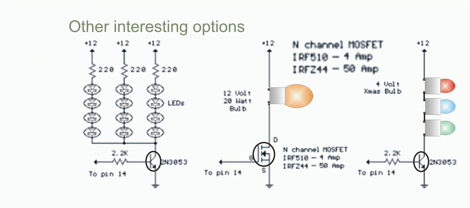
The circuit employs two strings of series connected lamps. One string is complimentary to the other, this means that when one string fades the other string gains luminescence. Two power transistors 2N3053 are connected in complimentary mode as shown in circuit 1. The collector of the first transistor is connected to base of the second one through a 2.2K resistor.


Different type of light source can be used by calculating the line current and bias voltages. Christmas tree bulb is a good option, as this bulb takes 200mA at 4V DC.


Three numbers in series thus do not require any current limiting resistance when applied voltage is 12V DC, as shown in the circuit. 2N3053 can smartly handle up to 500mA of current and hence using the same transistor three strings of LEDs can be connected in parallel with a current limiting resistance of 220ohm, as shown in circuit 2.


Four LEDs will be connected in a string, each LED chain will draw around 20mA of current. Hence, in practice, using the same transistor it is possible to connect nearly 12 to 15 strings in parallel that would draw a current of 240 to 300mA.

The principle of fading is designed around a quad OP-AMP LM324. One section of the IC is being used as a ramp generator, whereas the other section is used as a Schmitt trigger oscillator, for pleasure of vision the frequency of the ramp has been kept at 75Hz. In fact, the ramp circuit is the mother of all modern Pulse Width Modulation (PWM) circuit.


When a ramp is compared with a varying DC level, the output is pulse width modulating. This is conceived through simple geometry.


The frequency of the ramp is determined by the capacitor connected as shown by changing the values of the capacitor, the ramp frequency can be adjusted.

Instead of a NPN power transistor a MOSFET like IRZ44N is a good option. Such N channel MOSFETs are very smart and with a very nominal heat sink can handle much higher current than the NPN transistors.


This particular MOSFET is designed for a line current of 44 to 50 Amp depending on the junction temperature.

However, with proper heat sinks if the temperature rise is well monitored then such MOSFETs can smartly handle the current of 10- 15 Amp without any failure. While using MOSFET it is advisable to remember the power supply to the system should not go below 10V DC, as MOSFETs need a gate drive of 10V.


How to build Automatic 12 Volt Lamp Fader

How to Build Long Loopstick Antenna

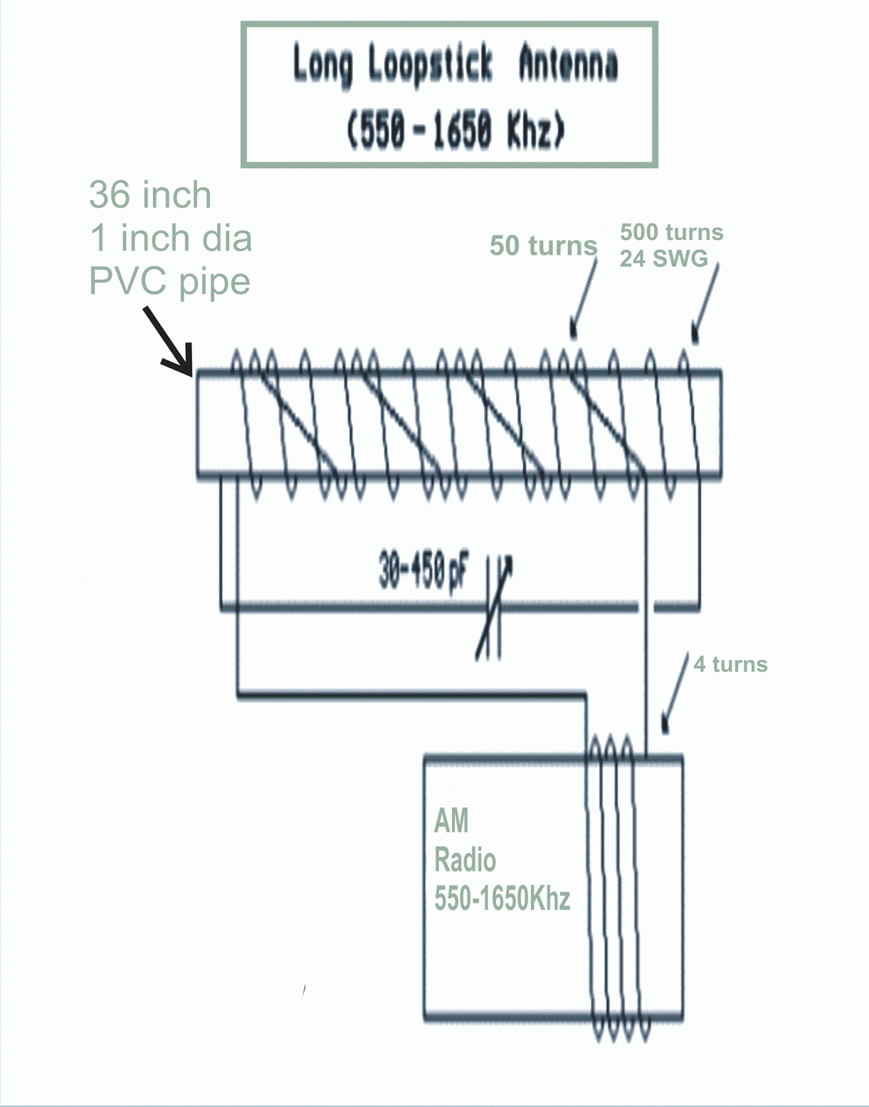
It is sometimes disturbing to have a AM radio in a countryside and not being able to get the reception clearly. It is simply because of the distance of the radio station and also the strength of the station. The only solution is to attach a powerful antenna to the receiving radio the uniqueness of the antenna lies in its simplicity and cost. The basic knowledge of making an antenna is there in the back end.

Generally, the frequency range of amplitude modulation in 560 to 1650 KHz in order to resonate the LC circuit that that is the antenna (2Ï€fL=1/(2Ï€f_c ))
4Ï€f^2 LC=1.Using this formula and using a 30- 450 pF gang condenser the handy inductance built on a 350ft long PVC pipe works quite well.
The inductance built around a PVC pipe is basically an air core inductor, the inductance of which is govern by the formula L=(R^2 N^2)/(9R+10l) where L is inductance in μH, R is coil radius in inches, l is coil length in inches and N is number of turns. The calculated inductance in tune with 33 pF- 330pF tuning capacitor should be around 250uH. Honestly with the proper geometrical calculation of winding a 3ft long PVC pipe an inductance value of 170uH is expected but in practice the inductance came out to be 213μH because of winding and error in winding spacing. The number of turn was around 500 and standard wire gauge of the wire 24. A secondary coil having 50 turns on the top of the primary was connected to the 4 turns of wire wound directly in the radio itself. His is to be noted that orientation should be such that the internal antenna of the radio should be co-axial with the external winding. Instead of this if you are allowed to open the radio set a few turns of the external antenna needs to be wound on the rod antenna of the radio. The best result is achieved when this tailored antenna is in perpendicular direction to the radio station and to be kept horizontal to the ground. The methodology of tuning the antenna is quite interesting. Firstly we need to select a very weak station of the AM band co that you hear sufficient amount of noise, at this point of time it is advisable to tune the gang condenser (antenna capacitor). Finally slight amount of physical adjustment of the rod maybe helpful. The electronic appliances, those have TRIACs , high voltage transformer, SMPs, high frequency devices may create electrical interferences and that is a concern, the antenna should be kept away from them.


How to Build Long Loopstick Antenna

Whistle Remote Control Circuit - Appliances ON/OFF through Whistle

For a hobbyist, it has always been fun to activate or automate through a clap or a whistle. A whistle sometimes can act like a voice recognition actuator as the frequency varies from person to person. However, for this use the tuning is to be done around 1700 Hz, a pitch that is somewhere near to the middle C octave of the piano chords. A condenser microphone acts as the audio sensor and produces a few milli - volts of current to activate the electrical actuator like a relay. For this it has to be supported by a transistor or FET.

Driving such a switch with the resultant milli-Volt from the condenser microphone is not possible. Hence an overall gain 4000 times larger is needed to be divided into two amplifier sections having gain values of 65 each.
Resistors denoted by the values R1, R2 and R3 are responsible for the individual gain of the amplifiers and are 1.1K, 1.2K and 15K respectively. Thus we arrive at the formula given below 


· R1 = Q/(G*C*2*Pi*F) = 8/(65*.01^-6*6.28*1700) = 1152 or 1.1K
· R2 = Q / ((2*Q^2)-G)*C*2*Pi*F) = 8/((128-65)*.01^-6*6.28*1700)= 1189 or 1.2K
· R3 = (2*Q)/(C*2*Pi*F) = 16/(.01^6*6.28*1700) = 150K


While choosing the resistor values for the proposed whistle remote control circuit, the quality factor (Q) has to be kept in mind. Q has to be greater than the square root of gain divided into two parts. It is a ratio of the central frequency and the band width. For this particular case, Q should have a value around 8.
It is to be noted that for a gain around 65 (the gain of individual amplifiers has a minimum value of 5.7), the quality factor has to be more than 5.7. Both capacitors employed in the amplifier need not have the same value, but for ease of calculation it can be kept at 0.01 microfarad. These particular values of capacitance are usable at audio frequencies and are readily available.
The op-Amps are biased in such a way that they are kept at nearly 50% of input supply (12 Volt DC). This is achieved by putting 10K resistors as potential dividers.
Output stage two rectifiers are fed into a capacitor (1 microfarad) which is connected to the base of a NPN transistor commonly denoted by 2N3904 or equivalent). Two resistors (2.7K and 3.3K) are used to bias the emitted voltage at 6.6 V. This enables the transistor to conduct a trigger for the flip-flop circuit when the peak value of the signal through the filter overtakes the combination voltage of the emitter 6.6V plus the emitter base voltage drop 0.7 V and the drop across a diode (0.7 V). If the clock circuits need to be triggered at a lower voltage than what it has set in the particular circuit, a 2.7K and a 3.3K resistor combination has to be altered. This will in turn determine the 6.6V DC input. Minor adjustments are possible like replacing the 3.3K resistor with a 5K. For the flip flop circuit IC number CD4013 is employed. This is basically a dual D type flip flop with recommended operating voltage between +3V DC to +15V DC.


Circuit diagram of the proposed whistle remote

 Whistle Remote Control Circuit - Appliances ON/OFF through Whistle

FM Beacon Broadcast Transmitter (88-108 MHz) Circuit

Frequency modulated broadcast band of 88 Mhz to 108 Mhz shall be used to transmit an audio tone. A distance of 100 yards is a working distance for such a broadcast band to be used by this circuit.


A popular timer 555 is being used to produce the tone that is nearly 600 Hz. The frequency modulates a heartly oscillator. The oscillator frequency is governed by an inductance and a capacitance.

The inductor is primarily an air core inductor which is built around a G.I. or M.S. bolt having 3*16 inches diameter. The bolt is basically a plain Hanger bolt termed as #8x32. Five turns are wound on the bolt and then the bolt is carefully removed by unscrewing.

After the coil is made it is stretched to 3* 8 inches and tapped at the centre. The frequency of the oscillation should be kept for best results at the centre of the band, i.e. 88 to 100 MHz. This can be shifted high or low by expanding or compressing the inductance coil. The 555 timer which produces the tone of around 600 Hz modulates the heartly oscillator. The output from the J-FET (2N4392) has the same phase as a signal at its gate and has the same voltage as input, where as the current is being amplified and thus acting as a current buffer.

A small signal diode (IN914/ IN4148) is being used here as a varactor Diode. This varactor diode is also termed as variable capacitor diode or variable reactance or variable cup diode whose capacitance varies as a function of the voltage across its anode and cathode and thus also being termed as a tuning diode. The total capacity in parallel with the inductor varies at the audio rate causing the oscillator frequency to change accordingly.

The ramping wave at Pin 2 and 6 of the timer circuit is being applied to the reverse bias diode through the IM resistance. This enables the capacitance of the diode to change as the ramping voltage changes. This alters the frequency of the tank circuit. An alternative methodology could have been employed so that an audio signal is fed to the IM resistance to modulate the oscillator but it would have required an additional pull up resistance to reverse bias the diodes.

The principle of the varactor diodes is very interesting as they operate in reverse bias condition. The thickness of the depletion Layer varies with the applied voltage and despite that there is no current through it. Its capacitance varies with the applied voltage. Actually the thickness of the depletion region varies to the square root of the applied voltage, as capacitance is inversely proportional to the depletion region thickness.

All components used in the circuit are readily available from radio shacks. The J-FET transistors must be of high frequency response.


FM Beacon Broadcast Transmitter (88-108 MHz) Circuit

120 VAC Lamp Dimmer Circuit

A lamp dimmer circuit can be conceived in so many ways but the challenge is cost effectiveness and reliability. Thyristors (or SCRs) and TRIACs are the major components associated with the lamp dimmer circuit.


Direct on line (120 VAC) dimmers can be configured either by two TRIACs connected anti parallel or it can be configured by 4 number of SCRs in the same topology for a full wave phase control. But this is a costly methodology.


The full wave phase control topology, as shown in the circuit was found in a RCA (Radio Corporation of America) power circuit book,1969. In fact, so far as power circuit is concerned, this is one of the cheapest effective typologies.


A full wave rectifier bridge is being employed in series with the AC line along with a SCR, the rectified AC also had its zero crossing.


The frequency of which is double that of the supply line and hence commutation of SCR at its natural zero is possible. Apparently it may appear that the SCR is working on a DC line but that is not the truth.

Two small transistors are connected as shown in the circuit. A 2.2 micro Farrad capacitor is employed in such a way so that when the voltage on the capacitor reaches about 8V the transistor will switch on.

As soon as the transistor is switched on, they discharge the capacitor through the SCR gate causing it to conduct.


As natural zero crossing phase is embedded in the topology, the conduction of the SCR is not a problem.


The 50K variable resistance is employed to adjust the time required for the capacitor to charge up to 8V. As the resistance is reduced, the time reduces and the SCR shall conduct at an early time at each half cycle. 


This applies more voltage across the load. Hence the 50K resistor can be used as a steering of the Dimmer circuit.

A standard SCR having 400V rating or above and respective current rating according to the load shall be a handy choice for this circuit. The whole circuit can be accommodated inside a match box size cabinet. A multi turn radio potentiometer of 50K value can be mounted on top of the box.


With the resistance of the potentiometer set to minimum the SCR shall only trigger when the supply voltage rises above 40V that is equivalent to 15o of the full cycle.


The 15K resistor plays an important role as it determines the setting of the capacitor voltage of 8V mostly.


If we increase the value of the resistance from 15K to higher value, that shall reduce the setting of the potentiometer (50K) for minimum opposition. It is a caution for the hobbyist not to touch any electronic component while the power is given, as the components are on direct supply mains.

12 Volt Lamp Dimmer Circuit Using 555 IC

The post details a simple 12V lamp dimmer circuit using IC 555.

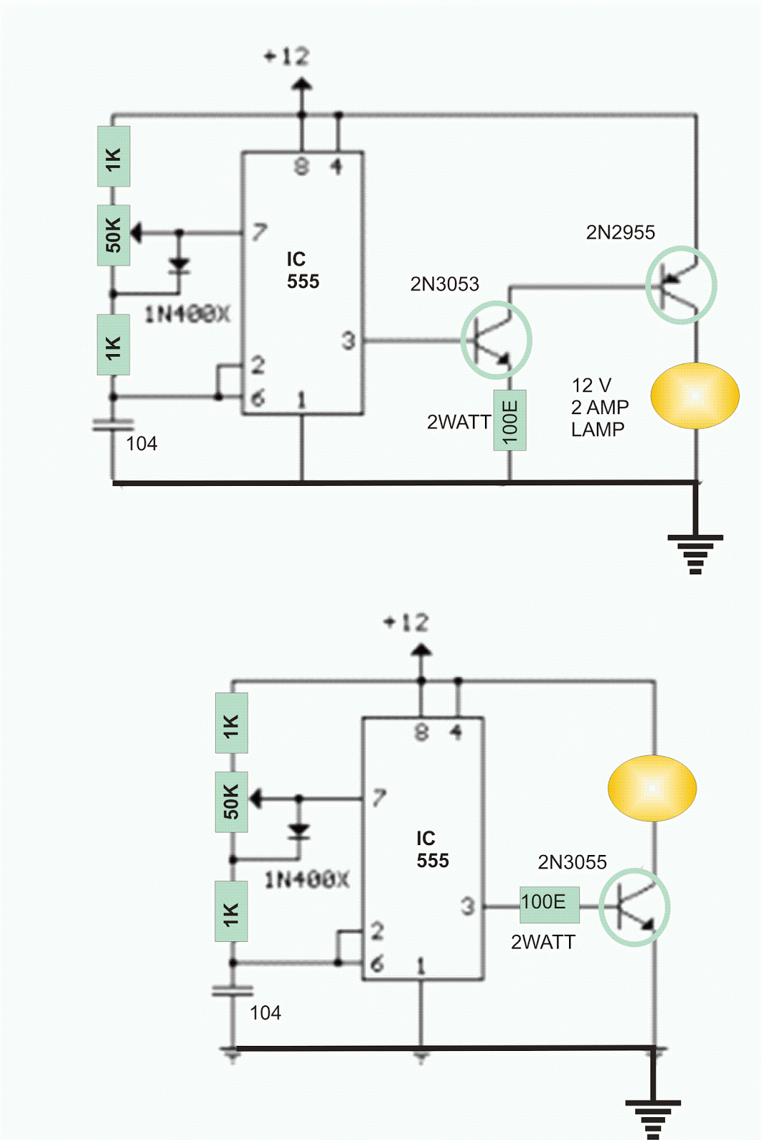
Lamp dimmer circuit is always a delight for the hobbyist. Here in this case, a 25W automobile lamp is being used as a dimmer element.


The lamp draws around 2 Amp of DC current. Hence for driving this bulb we need transistors those can handle such current.


In circuit 1 we have used primarily a PNP transistor 2N2955 to drive the bulb. This PNP is being biased by NPN transistor 2N3053, the base of which is triggered by a 555 timer.


The potential divider chain employed in conjunction with the 0.1 microFarrad capacitor produces a 200Hz square wave, the duty cycle of which can be varied by adjusting the 50K trimpot to an extent of 95% from 5%.


In circuit 2 the 2N3053 transistor is being omitted and instead of a PNP transistor a power transistor (2N3053) is being triggered by pin 3 directly.


A resistance of 100 ohms is being employed between pin 3 and base of the transistor. In case there is any gain oriented malfunction then a Darlington pair may have to be considered.
12 Volt Lamp Dimmer Circuit

Simple Triangle wave, Square wave Generator Circuit

In tnis post we learn a simple circuit idea which may be used for producing important waveforms such as triangle waveform and square waveform.

Triangular wave forms and square waves are the most sought after wave forms for the electronic hobbyist. Triangular wave forms are needed to develop PWM circuits.


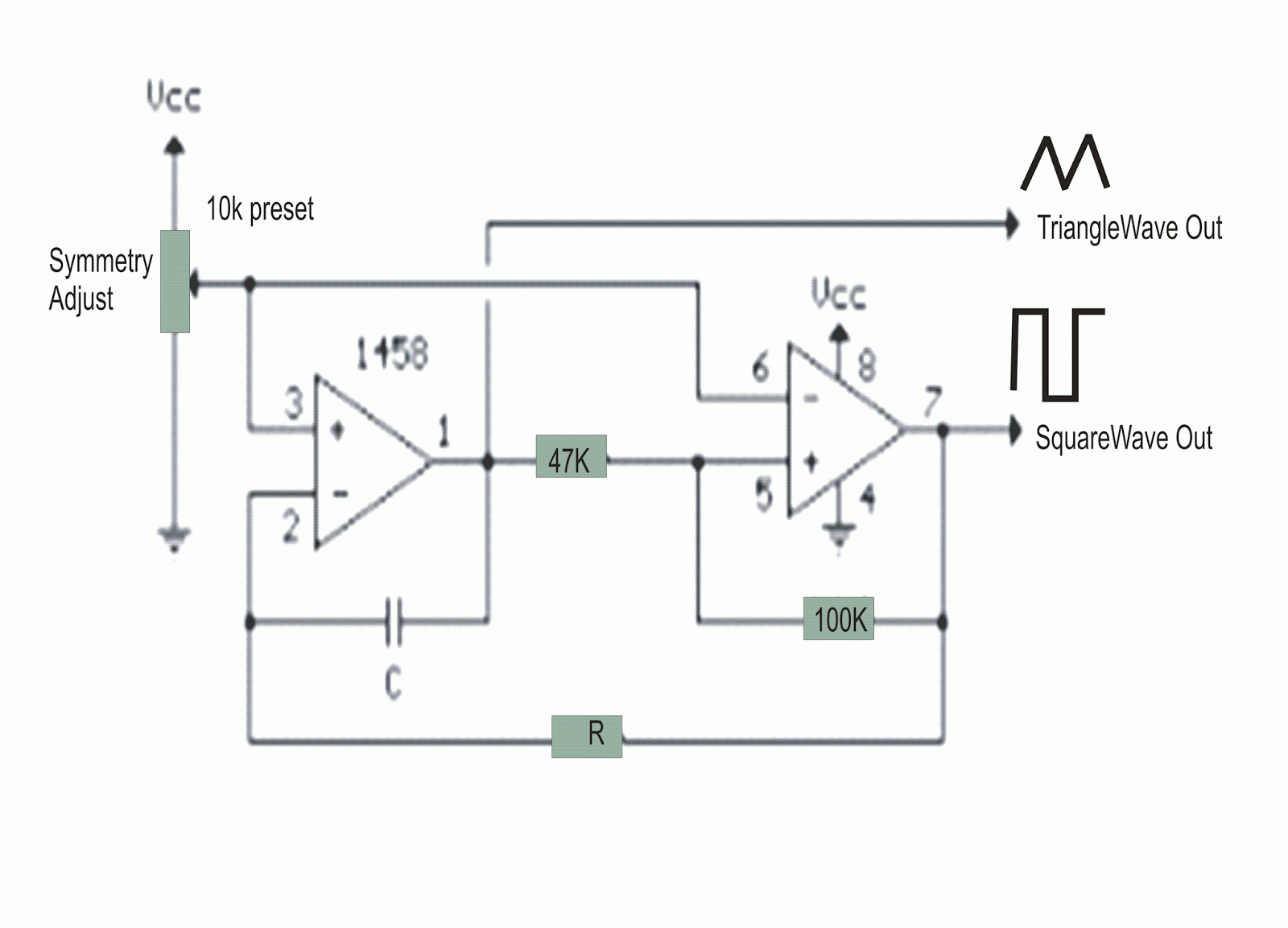
Both triangular and square wave forms are the tools for any electronic calibration. Here in this circuit by using a simple dual op-Amp, it is possible to get both the triangle and the square wave from the same circuit.


The amplifier at the left generates the triangular wave form. The frequency of the triangular wave shall depend on the value of the capacitance and value of R.


The time interval of one half-cycle is equal to R*C and it can source around 10mA of current at its output.


The output of the first op-Amp is being gated at the non- inverting input of the second op-Amp which has a symmetry adjustment pot connected at its inverting input. The output of the second op-Amp is a square wave.

The amplitude of the triangular wave form can be changed if we change the value of 47K resistor. You shall find the offset at the square wave output and this can be removed by putting a capacitor in series with pin 7.
 Simple Triangle wave, Square wave Generator Circuit

Make this Electronic Ignition Circuit

The post explains a how a simple IC 556 oscillator may be used to create a simple electronic ignition system.

Standard automotive ignition coil has been used in conjunction with a dual timer 556 and MOSFETs employed to handle the power. This can be termed as an electronic ignition. In the dual timer section one half is being used for frequency generation and the other part switches the oscillator section with breaker points getting “closed” and “open”. .

The frequency generator section in this circuit produces a rectangular waveform having frequency of 200 Hz. that drives the MOSFET. IRF 740 has a V-dss of 400 Volts and I-d of 10 Amperes sufficient margin in terms of Voltage and Current rating shall keep the switcher cool and efficient.

Pin 8 and pin 12 are being driven by the breaker contact that in turn produces an inverted signal at pin 9. As pin 9 and 4 have shared logic state, this determines the state of pin 5 that drives the FET.

The frequency determining elements are 15 K, 4K7 resistors and 0.33 micro- Farad capacitor. The duty cycle is 4 milli seconds on the +Ve and 2 milli seconds for the –Ve . During positive transition the FET gates are high enabling the ignition coil current to rise to 4 Amperes level. A Burst of 80 milli Jules of Energy is released in the spark plug when the pin 5 goes to ground state thus turning off the switcher.


A 12 volt Zener Diode as shown in the electronic ignition circuit ensures that Voltage at FET Gate does not go below -0.7 V or above +12 V. A 200 Volt , 5 watt zener is employed to lengthen the Spark Gap. A shorted plug shall work with this circuit however, care must be taken to suppress voltage transients by using MOVs or TVSs such as 1.5KE200A in place of the Zener or in addition.

Make this Electronic Ignition Circuit

How to build Analog Milliamp Meter Used as Voltmeter

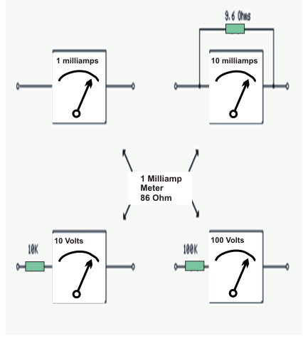
A milli Amp analog meter often used along with audio system can be easily converted into a decent volt meter, all that is needed is an understanding of the requirement and the meter.
In case a 10V full scale meter is to be designed, then a 10K resistance is to be put in series with the meter coil so that for an applied voltage of 10V a meter can receive 1milliAmp only. The meter itself has an internal resistance and if that is measured properly then in actual practice the resistor to be connected in series shall be having a value of 1000 ohms – IR (internal resistance of the meter). When we measure smaller voltage then this internal resistance of the meter plays a significant role, say for this particular case the internal resistance is 86 ohms, hence, for a I.V. full scale meter the value of the external resistance would be (1000-86) 914 ohms.


How to build Analog Milliamp Meter Used as Voltmeter


The milli amp meter can also be used as an Amp meter of higher currents by adding shunt resistances. This is being achieved by simple networking methodologies if we want to change the meter to a 10milliAmp instead of 1milliAmp meter we need to add 9.6 ohms in parallel to the meter coil to convert the meter to a 10milliAmp full scale meter.

Reverse Lamp Dimmer Circuit for Simulating Sunrise Effect

The post explains a simple automatic mains lamp reverse dimmer circuit which can be used to imitate a sunrise effect.

A sunrise simulator lamp is a modified version of a dimmer circuit. 120V AC lamp is connected to a bridge rectifier that supplies DC though there is no functional difference as the lamp is passive and being resistive in nature there is no operational problem.


The circuit is made such that the lamp illuminates over a period of 20 minutes. The lamp is connected in series with a N channel MOSFET.


Here in this case IRF 640 having a V -DS of 200V and I of 11Amp at 100oC or an IRF 740 having V-DS of 400V and Id of 6.3Amp at 100oC is recommended.


However, for a 120V supply IRF 740 is a better choice. A current limiting resistance is employed in series with the lamp. The lamp has a drawing current of 500mA that determines the wattage of the current limiting resistance.


LM324 a quad OP-Amp is employed for the multiple stages required to build the circuit. A triangular wave form of around 700Hz is produced at pin number 1 and a slow variable DC voltage is generated at pin number 8.


These two voltages are compared in the last stage of the op-Amp. This stage is acting as a comparator.


Quite naturally the comparator generates varying duty cycle. This is the parent methodology of generating PWM wave form. This PWM signal shall trigger the MOSFET and start illuminating the bulb within sixty seconds of powering up. And the full illumination is reached over a period of 1/3 of an hour.


This period can be adjusted by varying the resistance connected to pin number 9. The current limiting resistance of 2.2 ohms along with the capacitor of 0.015microFarrad connected across it also acts as a RFI suppressor.

Before each operation, there should be a minimum interval of 5 to 10 minutes. During this time the 3300microFarrad capacitor gets discharged through the 10K resistor and the diode connected with it. As the circuit is connected to main supply, caution should be taken while in use.


Reverse Lamp Dimmer Circuit for Simulating Sunrise Effect

Digital Voltmeter Circuit

In this post we learn about a simple 3,1/2 digit digital voltmeter circuit.


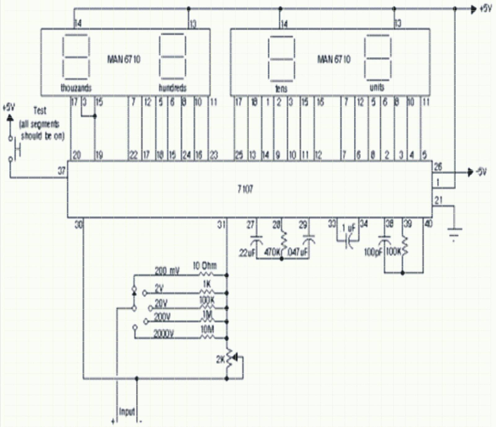
IC7107 is the most common and economic analog to digital converter available in market. It can convert an analog signal to 3 digit LED display.

The displays are seven segment LEDs (8). 7107 has a build in reference and a clock along with seven segment decoder and display driver.

The simple connectivity as per the circuit shall ensure a reliable A to D converter worth display. The power supply employed is +5V DC.

The input for this particular circuit could be any voltage up to 2000V. It is imperative to mention in this context that the highest displayable voltage is 1999V.

The input is being introduced between pin no. 30 & 31 through a parallel rung of resistors namely 10Ω, 1KΩ, 100KΩ, 1MΩ, 10MΩ for selection of ranges of 200mV, 2V, 20V, 200V and 2000V.

A push to on switch is connected between +5 V DC and pin no. 37 to check the health of all the segments of four displays.

The resistor used here are all quarter watt and the seven segment displays are common anode type.

It is advisable to download the data sheet of 7107 and use the recommended components.

The resistors need to be of 1% tolerance type for best result.


Digital Voltmeter Circuit

Blown Fuse Monitor Circuit

The post explains a simple fuse monitor or indicator circuit, for indicating the fuse status anytime.

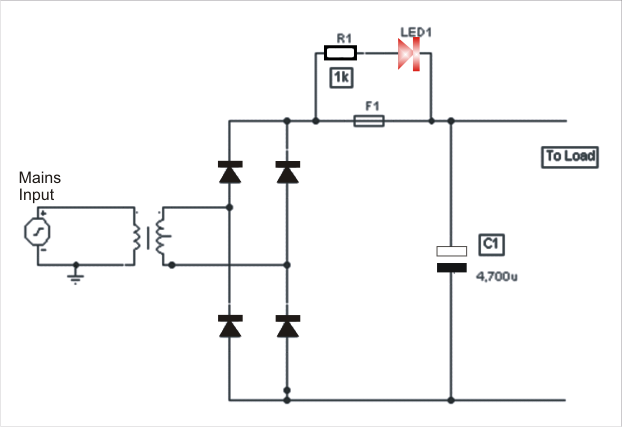
This is one of the simplest yet effective alarm cum monitor for detecting any blown fuse. A resistance of value 1K is placed in series with a LED and connected across the fuse which is to be tested.


Normally when the fuse is healthy, LED 1 will not get any bias.


Thus, it will not raise an alarm. However, the moment the fuse is blown, LED1 gets a feed in bias and starts to glow.


The value of the resistor R1 and its wattage should obviously be decided depending on the type of LED and the supply across it.


Suitably connecting a 12V zener and a 12V electronic buzzer across the fuse can enable an audio output (alarm sound) if so required.


Blown Fuse Monitor Circuit

Simple Field Strength Meter Circuit

A simple field strength meter circuit is presented in this article, let's learn more about it's construction details.
For a radio receiver, it is often a pain to evaluate the strength of the field on which the performance of the radio is dependent.


The circuit used for this purpose is a cost effective yet useful tool to achieve performance evaluation of the radio field strength.


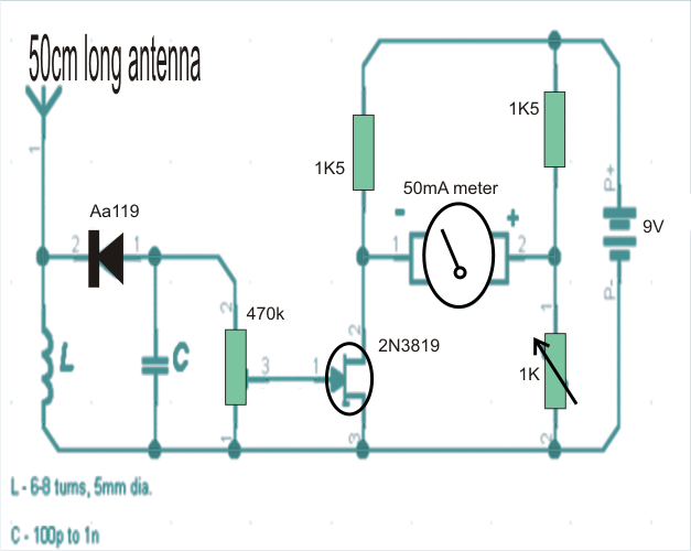
The extreme left of the circuit is the crystal receiver or crystal radio part of the circuit. A suitable germanium diode like the IN34 or AA119 is recommended.


A silicon diode does not achieve the performance of a germanium diode for its functions as a varactor because of its depletion layer characteristic.


The inductance can be built by 6 to 8 turns of enameled wire having a diameter of 1milimeter and a coil diameter of millimeter.


The capacitor selected is around 100picoFarrad that resonate with inductance. By adjusting the spacing of the turns, the frequency can be varied.


The second stage of the circuit employs a high impedance amplifier in the style of a JFET 2N3819 that is gated by a variable 470K resistance.


This is basically a potentiometer. By adjusting this, the sensitivity of the circuit is adjusted. This trimmer is used for achieving 0 deflection in the meter.


It is recommended to use meters of 50miliAmpere or lesser capacity.

While calibrating with different antennae, this meter is very useful. However, great performance from such a simple circuit with a cheap meter is not expected.


 Simple Field Strength Meter Circuit

Making a Home Theater System Using IC TDA 7560

The TDA7560 is a breakthrough BCD (Bipolar / CMOS / DMOS) expertise class AB Audio Power Amplifier in Flexiwatt 25 package designed for superior power car radio.
The fully complementary P-Channel/N-Channel output structure makes it possible for a rail to rail output voltage sway which, fused with high output current and minimized saturation losses sets new innovative power referrals in the car-radio field, with incomparable distortion performances.

DC OFFSET DETECTOR

The TDA7560 combines a DC offset sensor to prevent that an anomalous DC offset on the inputs of the amplifier might be multiplied by the gain and lead to a risky significant offset on the outputs that may result in speakers harm for overheating. The feature is enabled by the MUTE pin and operates with the amplifier umuted and without signal on the inputs. The DC offset identification is signaled out on the HSD pin.

STAND-BY AND MUTING STAND-BY and MUTING facilities are both CMOS-COMPATIBLE. In lack of genuine CMOS ports or microprocessors, a direct connection to Vs of these two pins is suitable yet a 470 kOhm equivalent resistance need to present between the power as well as the muting together with stand-by pins.


 Making a Home Theater System Using IC TDA 7560

Making a Simple 1.25 to 35v Variable Power Supply Circuit Using IC LM338

The LM138 series of variable 3-terminal positive voltage regulators is capable of supplying more than 5A over a 1.2V to 32V output range.
They are surely particularly easy to utilize and need just 2 resistors to make the output voltage. Mindful circuit theme has led to outstanding load and line regulation—comparable to a number of commercial power supplies.

The LM138 range comes in a conventional 3-lead transistor package. A unique feature of the LM138 family is time-dependent current restricting.

The current constrain circuitry enables highest currents of up to 12A to be sucked from the regulator for quicker time frames.

This permits the LM138 to be used with excessive transient loads and accelerates start-up under full-load setting.

Under repeated loading situations, the current limit reduces to a harmless value safeguarding the regulator. Furthermore featured on the chip are thermal overload safeguard and safe space coverage for the power transistor.

Overload resistance continues practical despite that the adjustment pin is accidentally turned off. Ordinarily, no capacitors come together unless the unit is situated greater than 6 inches from the input filter capacitors in which instance an input skip over is used. An output capacitor may be combined with build up transient response, when bypassing the adjust


'
Making a Simple 1.25 to 35v Variable Power Supply Circuit Using IC LM338  
 
                                                                          Courtesy: http://www.ti.com/lit/ds/symlink/lm138.pdf

Simplest Single Phase Preventor Circuit for Three Phase Motor Potection

For a 3-phase induction motor,Lit is necessary that all the three phases of supply are present while it is on load.

When any one of the fuses goes out, or a phase is missing, the motor will continue to run with two phases only, but it will start drawing a huge current for the same load. This high current may ruin the motor, unless switched off immediately. A single phase preventor circuit avoids such a mishap. With this circuit the motor will not run, unless all the three phases are present. In a 3-phase supply, the voltages are 120 degrees apart from each other. Thus the addition of three phases gives zero voltage. lf any one of the phase goes, voltage present at the summing point equals half the line voltage. ‘ In this circuit, the three phases (R, Y, B) are connected to line neutral, which in turn is connected to the ground of the circuit. When all three phases are present, voltage at point D is zero.


 So potential at pin 3 of 1C 741 is also zero, but voltage at pin 2 is nearly 4V. Here 741 is used as a comparator and the voltage at pin 6 is zero. Hence the relay cannot operate. When a phase goes out, voltage at point D goes up to about halt the line voltage. This voltage is divided by 150k and 50k resistors. The voltage at pin 3 is about 8V when 50k potentiometer is properly adjusted. The voltage at pin 6 is about 12V. This base voltage can drive the relay into operating condition. So, the relay would operate when any of the phases goes out. This relay, when used in the control circuit of the 3-phase motor, or with a circuit breaker, would switch the power oft on operation.


Simplest Single Phase Preventor Circuit for Three Phase Motor Potection

Piezo Buzzer Driver Circuit Diagram

Buzzers are small, light, simple to use, and yet provide a loud output signal. They are either of the passive or of the active type.
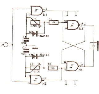
The former are driven by an AF signal source, while the latter feature a built-in oscillator, and require a direct voltage only. This circuit is a double AF oscillator for driving passive buzzers. It ensures a richer out- put sound than normally obtain- able from a piezo buzzer due to the use of two oscillators, N1 and N2, whose output signal lies between 1 and 10 kHz. Gates Na-N4 form an S-R bistable which is controlled by the out- puts of N1-N2, and drives the buzzer direct.
Optimum effects are achieved when a simple ratio is set between the oscillator frequencies, e.g. 3:4.
Piezoelectric resonators, also referred to as buzzers, are frequently used for providing audible signals in all sorts of electronic equipment. 


The spectral l composition of the output X signal is fairly complex, due to the presence of both the fun- damental notes and the differ- ence and sum frequency.
The timbre so obtained varies as a function of the ratio between the oscillator frequencies, which are adjustable with the aid of presets P1-P2. Note that diodes D1-D2 reduce the duty factor of the oscillator signals to about 25%.
The resulting waveform is always composed of rectangular signals, but these differ in respect of their period to ensure that the buzzer pro- duces a rather agreeable sound. The buzzer driver is controlled by a logic level applied to point X. The quiescent current consumption is virtually negligible, while about 10 mA is drawn in the actuated state. 


Buzzer Driver Circuit Diagram


Piezo Buzzer Driver Circuit Diagram

Adjustable Voltage, Current Power Supply Circuit Using IC L200

IC2 is connected as a differential amplifier and compares the signals at its two inputs.
Referring to the circuit diagram: the input comprises a mains switch, fuse, transformer, bridge rectifier and smoothing capacitor (C2). 


The difference between the inputs is the voltage drop across 'current’ sensor R4. This IC feeds the current sensing input (pin 2) of the L200. 


P1 in the feedback loop of the 741 is used to vary the output current of the circuit. IC1 must be mounted on a suitable heat sink as it dissipates nearly all the power of the circuit.
The reference level output from I pin 4 of IC1 goes to the voltage divider made up of R5 and P2 (this pot sets the value of the output voltage).


The power supply can quite easily be built into a case and a voltmeter and ammeter mounted on the front panel. ln view of the accuracy of the circuit these should ideally be digital meters, but virtually any type will do.


If you compare the expense and the rating of this power supply you will get a surprise, because the output voltage and current are fully adjustable between O. . . 18 V and 0 . . . 1.8 A respectively and costs have still been kept very reasonable. 


Diode D5 and capacitor C1 produce a negative auxiliary voltage, which is stabilized by zener diode D6 and capacitor C4. 


All this is necessary to enable the output voltage to be adjusted down to zero volts. During the construction of this part of the circuit bear in mind that the positive lead of electrolytic capacitor C4 is connected to earth! Regulation is provided by IC1 and IC2. Capacitor C3 suppresses any residual transients at the input of lC1 and it should therefore be connected as closely as possible to IC1 similarly C4 and IC2). 


The negative voltage provides the negative supply for the two ICs.


 Adjustable Voltage, Current Power Supply Circuit Using IC L200

AC Mains Voltage Stabilizer Circuit

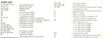
It will be easier to understand the operation of the circuit if we separate the under and over-voltage protection circuitry comprising transistors T1, T2 and associated components from the rest of the regulator circuit. Diode Dl arid. capacitor C2 provide 24V DC supply required to operate the relays. 

Diode D2 and capacitor Cl provide the sample DC voltage for generating reference voltages for the cutout. For initial setting of cutout, collector of Tl is not connected to the base of T2. Also the time delay capacitor C4 is only connected after both under- and over- voltage points have been preset independently. Initially, due to the potential divider action of resistors R4, R6 and preset VR2, a voltage would appear at the base of T2. · lf this voltage is 0.6 ·V or more above the zener diode voltage of D4, transistor T2 would conduct, energising the relay and connecting the hot tap of the auto-transformer to the universal socket’s hot terminal through N/O contacts of the relay RLl. 


 Resistor R7 is for limiting base current. Therefore poten- tiometer VR2 is preset in a position where the relay would just switch off below the required lower trip point. On the sample prototype this was adjusted at l55V input, a value at which the output voltage of the regulator was 200V—the lower limit for our specified regulated output. Whenever output voltage goes below this safe operating voltage, the relay releases and disconnects the power to the appliance and simultaneously gives a visible indication of this by applying power to the neon light through its N/ C contacts. At this point the collector of Tl is connected to the base of T2. Again a sample voltage would be available at the cathode of D3 due to the potential divider action—of Rl, VR1 and R3. If this voltage exceeds the zener voltage of D3, transistor T1 would be able to conduct. This would clamp the base of T2 to ground.

 Since the base ofT2 has been pulled to ground, T2 would be no longer conductive and hence once again the cutout relay would be released, disconnecting the supply to the load. Preset VRl is so adjusted that as soon as the output supply voltage exceeds the upper limit (240·volts in our case), transistor T1 conducts and releases the relay. Once the over- and under-voltage points have been set, capacitor C4 (whose value may be found out experimentally) may be added between the base of T2 and ground. This capacitor is essential to introduce a time lag in the operation of the cutout when rapid variations occur in mains supply. With capacitor C4 connected, the cutout waits till a steady level of voltage is reached. This also helps in avoiding erratic behaviour of the cutout. Referring to only one section, say around T3 and T4, of our regulator circuitry, we find that transistor T3 would conduct when its base is at a negative potential as compared to its emitter. The emitter of T3 is fed with a fixed reference voltage from the anode of D5 which remains more or less constant over the input voltage range. 

Preset VR3 is adjusted to a point where, any further increase in the input voltage switches T3 on, and consequently T4,·pulling_ RL2 on. Further stages are similarly set at different voltages. Setting Having checked up the wiring, procure a variable auto- transformer (known as variac) to set the correct input-output voltage range. A very simple test for making sure that all stages of your circuit are operating is to feed input mains voltage and see that all the relays can be switched on or off by merely changing the settings of presets. At this stage no output load should be connected to the regulator. lf any part of the circuit remains permanently on or off, then the components as well as wiring for that particular stage may be checked thoroughly for faults. lf everything seems correct then connect a good quality multimeter, switched to read 250V AC, at the output socket. 

The cheap type of AC voltmeter mounted on the regulator panel is generally not a reliable instrument for accurate readings and should periodically be checked for calibration. Using a variac apply an input between 155 to 160 volts till you get an output just around 200 volts. Reduce this voltage slightly and make sure that as soon as it reaches below 200 volts (threshold between 195 and 200V) the low voltage cutout transistor T2 switches off, releasing RL1. For this test, base of T2 should not be connected to collector of Tl, so also positive of C4,_ as described under the cutout section. At this point no voltage would be available at socket SOI and neon Ll would be lit. Increase and decrease this voltage at the threshold range a number of times to make sure the steady repeat accuracy of the cutout. Having set this, preset VR2 may be sealed with a blob of paint. Next keep on increasing the input volts till the output just reaches 240V our upper limit for regulated voltage.

 Till this _ stage all the presets of the regulator must be so positioned that none of the relays is on. So far as the auto-transformer is concerned this would mean that the input hot line is connected to point 1 of the transformer with output at point 4. incidentally this is the maximum step-up given by the transformer for the lowest input range. As soon as output voltage tries to shoot beyond 240V, preset VR3 should be adjusted to switch on RL2. ` This would change the input hot end from point l to point 2 of X2, thus reducing the step·up ratio of X2. Keep on increasing the input voltage with variac till again it reaches 240V output. Now the relay RL3 should be adjusted with preset VR4 to switch on, further reducing the step-up ratio.


AC Mains Voltage Stabilizer Circuit

Simple Fish Caller Circuit

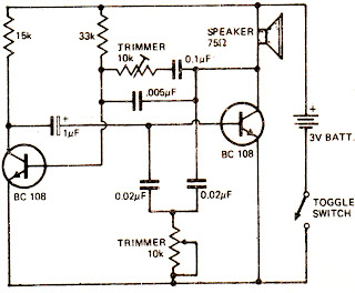
A lot of controversy exists among amateur fishermen as to the effectiveness of "fish-callers". Some swear by them, others just shake their heads. Here’s an inexpensive way of finding out. The two·transistor circuit drives the speaker. 

Varying the two potentiometers produces a wide variety of sounds. You may be lucky and hit on one that will bring in the big ones. An inexpensive waterproof housing is thick walled polythene bag with a few lead sinkers inside. An on-off toggle switch can be manipulated without opening the bag when switching power on and off. The bag opening is sealed with good quality electrical tape to make system waterproof. Tape seal should be renewed after each use.


Circuit Diagram :


Simple Fish Caller Circuit

Deriving High Current from 7805, 7812 Voltage Regulator Power Supply Citcuits

If, for instance, a power transistor is connected in parallel with the IC, the supply will no longer be protected against short-circuits. 

The circuit given here shows that a simpler solution is possible: the power transistor, T1, is provided with an emitter resistor! This effectively solves the problem, because the current through Tl is then proportional to the current supplied by the voltage regulator.

But this solution A suffers from a heavy power loss during short-circuit conditions, which is not really acceptable either. 

There are various ways and means of drawing more current from a voltage regulator IC than it was originally intended to supply, but most methods have their disadvantages.
lf the 7805 or 7812 regulator and T1 are mounted onto the same heatsink, the transistor is also thermally protected! The output voltage is dependent only on the type of voltage regulator used and, as drawn here, the circuit is suitable for currents up to 2 A. 

lf higher values are required, some components need to be changed according to the table. For currents above 7 A, transistor T1 must be replaced by two parallel-connected transistors each of which has an emitter resistor, R1 and R1' respectively.

That can, of course, be remedied by adding a current sensor in the shape of an extra transistor which, during overload conditions, cuts off the base current to the power transistor.
Deriving High Current from 7805, 7812 Voltage Regulator Power Supply Citcuits

Electronic Water Pressure Switch Circuit

A water pressure switch is designed for sensing pressure of an incoming water flow from a source which may be a booster pump, and compare it with the water pressure inside the tank which is being filled by the booster pump water flow. When the water pressure inside the tank crosses the set threshold relative to the pump pressure, an in-built switch is tripped. The trip switch is configured with the booster pump electrical such that when it trips, the motor halts and prevents the tank from filling above the desired upper threshold. A reverse action is initiated as soon as the water level in the tank reaches below a certain lower threshold.

Pressure switches are normally mechanical with their operations, and may not be easy to build or replicate at home by a hobbyist. Even an electronic equivalent of the same which might require a precise pressure sensor could be difficult to implement due to the many intricacies of the system.

However a simple alternative for fulfilling the above specified functioning of a pressure switch could be replicated with the help of the following shown electronic set up.

In the design we can see a small PVC container which could be a piece of plastic pipe cut into an appropriate size for the purpose.

A small water inlet derived from the main booster motor water supply is injected into the container and allowed to be filled and its level monitored relative to the main tank.

The container is required to be dimensioned such that the accumulated water level inside it proportionately corresponds to the water level of the main tank.


Electronic Water Pressure Switch Circuit


The upper threshold of the main tank and the container are monitored and the position marked over the container precisely corresponding to the upper cut-off threshold of the main tank.

This position is marked and fitted with a reed relay on the outer side of the container.

Another reed switch is clamped at the bottom of the container intended for the lower level switch ON purpose.

The inside of the container consists of a float embedded with a strong neodymium magnet, this float is intended to float upwards and downwards with the the water's rising or declining levels inside the container.

The above action in turn is intended to interact with the adjoining external reed switches creating a toggling response in them.


Electronic Water Pressure Switch Circuit

The reed switch contacts are integrated with a simple set-reset circuit as shown above. This set/reset latch configuration consists of a relay which is to be wired up with the booster motor electrical.

Referring to the above controller circuit, when the water level is below the lower reed switch, it toggles the circuit and sets the relay into a switch ON position activating the connected motor.

The motor starts pumping water into the tank and when the tank level reaches the maximum threshold the container level also correspondingly rises to the set upper level triggering the relevant reed switch2, which instantly switches OFF the motor.

The circuit keeps the situation latched until the water level has yet again reached the lower threshold of the main tank as and the container. The cycle is repeated consistently maintaining the desired quantity of water in the tank and preventing the motor from incorrect triggering and burning. 

Digital Voltmeter and Ammeter Circuit Module

This V/I display module is eminently suitable for building into an existing DC power supply, where it gives a precise indication of the set voltage or the current consumption of the load.
In the voltage range, the decimal point lights on LD3, and the resolution is therefore 100 mV Two current ranges are possible: 0-9.99 A (link a) or 0-0.999 (.999) A (link b).


The 3-digit readout is based on A/D converter Type CA3l62 and BCD-to-7 segment decoder Type CA3l6l, both from RCA.


The resulting small negative deviation in the volt- age range is compensated by P2.


These points should be adjusted in the above order. Two presets, P1 and P3, are required to ensure correct nulling of the module. P1 compensates for the quiescent current consumption of the regulator circuit in the supply.


When voltage measurement is selected, P4-R1 attenuates the input voltage by a factor 100. Also, point D is pulled low so that the decimal point on the LS display, and the
The current sensing resistor is therefore either 0Rl or lR0. It is important that Rs does not affect the output volt- age of the supply in question.


When current measurement is selected, the drop across the sensing resistor is applied direct to the HI-LO inputs of DAC IC1.


The sensing resistor has such a low value as to render the voltage divider ineffective. There are four adjustment points in the module: P1: current range nulling; P2: full-scale current calibration; P3: voltage range nulling; P4: full-scale voltage calibration.
The V/I display module is conveniently fed from the unregulated voltage available in the supply (max. 35 V) see points E and F in Fig. 2; bridge rectifier B1 may then be omitted.
It must, therefore, be fitted ahead of the voltage divider that controls the output voltage. DPDT switch S1 selects between l voltage and current readings.


 Circuit Diagram

Digital Voltmeter and Ammeter Circuit Module
 

Hi-Fi audio amplifier by ic TDA2003

This is the Hifi power amplifier circuit, will be used TDA2003 ic number. The normal operation of the integrated circuit,the music amplifier for car audio radio sound.Which it uses the supply voltage from 12 volt car battery.But this circuit adapted for use at home by listening to change power supply to 15 volts.
This allows a higher watt power than the existing 3watt RMS.The TDA2003 IC is protected from damage and short circuits,When the load over.Maximum Voltage of 28 volts, the frequency response 40 Hz – 15 kHz.


Circuit Diagram


Hi-Fi audio amplifier by ic TDA2003


When entering the power supply 15 volts to the circuit. The C1 coupling audio signal through the VR1 to adjust the volume.Then sent to the C2 anti-noise DC input signal to the pin 1 of IC.The non inverting amplifier circuit is a non-return phase.This is the signal output pin 4, by a C5 enhances the stability of low-frequency response the better.And noise will be dropped down to ground by R4 and C6 before output to speakers.Another part of the output signal, which is fed back through C3, and R1, to enter the pin 2 inverting.To maintain a constant frequency response at-3dB.And if you want to add. Frequency response is to reduce the C3.The C8 is a filter file before the operation.C7 cut out noise from the supply.If you want a stereo amplifier,Is to create an additional set.

Power Amplifier Genneral Purpose by IC TDA2030

This is Power Amplifier Genneral Purpose circuit,main part is IC TDA2030.
It is OTL Amp 10W rms at 8ohm.


Circuit Diagram:

Power Amplifier Genneral Purpose by IC TDA2030
 

The multi-purpose Amplifier using TDA2030

This The multi-purpose Amplifier using TDA2030. It is have power 8 watt (RMS) at 8 ohm loudspeakers. It is have low noise be valuable THD (Total harmonic distortion) 0.1% , When friends use Power supply Voltage Source 28 Volt at 4 ohm loudspeakers have output power 12Watt. But be high class the noise increases to are 2 times. Besides still three be usable with Volt supply about 9Volt , but there is the electric power is down respectively. The VR1 use for Volume popularity level of sound signal. By if a friend can’t seek 22K values use 50K values can replace. For other detail about the integrated circuit TDA2030 IC and other , friends see in the circuit better yes. 

Circuit Diagram:


The multi-purpose Amplifier using TDA2030
 

Inverter 12V to 220V 100W by Transistor

This circuit is 100 watt power inverter using power transistor 2N3055. It is designed for you that need to use appliances at outdoor or no electrical places. Someone use it in car or the high mountain etc.

The maximum output power of this circuit about 100 watts, it is suitable for a normal lighting (all home lamps), also used for radio, mini TV, stereo or someone use it for
 

How it works
 
From the schematic diagram in Figure 1 this circuit will include of 4 main section are:
1. The transistors Q1,Q2 act as the frequency oscillator circuit.
2. Both transistors Q3,Q4 act as the frequency divider circuit
3. The Q5,Q6 act as the driver circuit.
4. The Q7,Q8 act as the output circuit.

Let’s look at to both transistors Q1,Q2 will be connected together as the astable multivibrator form. It will generate the output frequency about 100 Hz at the collector lead of Q2. Then this signal will sent to the two frequency divider makes the frequency is reduced down about 50Hz

Cause we don’t design the circuit to directly work at 50 Hz. Because the generating the steady low frequency is very hard.

The output from divider circuit is sent to base of Q5,Q6. To increase current up to drive the output transistors Q7,Q8, then drive the transformer, finally to supply load.


Note:
1. Normally, use the 2-3A transformers for 20-30watt for the incandescent lamp. But use need 100watt use must use 8A transformer so expensive for me.
2. The primary coil of transformer use may use 9V CT 9V or 10V ct 10V or 12V ct 12V.
Which normal I use 12V ct 12V makes the output voltage about AC 220V (no load). But there is load voltage will reduce to AC190V
3.This circuit will has output as square wave form. So cannot use for inductor load.
4. This transformer, we may use secondary coil is the output voltage as you need, example we connects to the power amplifier that use AC 24 volts so we use AC 24V secondary coil etc.

How to builds.
It is like all our projects. To begin with make the PCB or you can use the universal PCB. Then, assemble all part on PCB as Figure 2. Next check all for error. Check again and check again.

Then apply the 12V 10A battery to this circuit and use the voltmeter to measure AC voltage output. Next connects load to the circuit. 


                          Figure 1 Circuit diagram of Inverter 12V to 220V 100W by Transistor


source:http://www.eleccircuit.com/inverter-12v-to-220v-100w-transistor/
 
Blogger Templates