Simple 1000W Power Inverter circuit
This is the power inverter circuit based MOSFET RFP50N06. The inverter capable to handle loads up to 1000W, it’s depended on your power inverter transformer. The RFP50N06 Fets are rated at 50 Amps and 60 Volts. Heatsink is required for cooling the MOSFETs. You may add some MOSFETs with parallel connection to get more power. It is recommended to have a “Fuse” in the Power Line and to always have a “Load connected”, while power is being applied.
Simple 1000W Power Inverter circut
40 LED Bicycle Light Circuit Diagram Using 555 IC
The 555 circuit below is a flashing bicycle light powered with four C,D or AA cells (6 volts). Two sets of 20 LEDs will alternately flash at approximately 4.7 cycles per second using RC values shown (4.7K for R1, 150K for R2 and a 1uF capacitor). Time intervals for the two lamps are about 107 milliseconds (T1, upper LEDs) and 104 milliseconds (T2 lower LEDs). Two transistors are used to provide additional current beyond the 200 mA limit of the 555 timer. A single LED is placed in series with the base of the PNP transistor so that the lower 20 LEDs turn off when the 555 output goes high during the T1 time interval. The high output level of the 555 timer is 1.7 volts less than the supply voltage.
40 LED Bicycle Light Circuit Diagram
Adding the LED increases the forward voltage required for the PNP transistor to about 2.7 volts so that the 1.7 volt difference from supply to the output is insufficient to turn on the transistor. Each LED is supplied with about 20mA of current for a total of 220mA. The circuit should work with additional LEDs up to about 40 for each group, or 81 total. The circuit will also work with fewer LEDs so it could be assembled and tested with just 5 LEDs (two groups of two plus one) before adding the others.
Circuit Source: DIY Electronics Projects
Voltage Inverter Circuit Using IC NE555
In many circuits we need to generate an internal adjustable voltage. This circuit shows how it is possible to use a trusty old NE555 timer IC and a bit of external circuitry to create a voltage inverter and doubler. The input voltage to be doubled is fed in at connector K1. To generate the stepped-up output at connector K2 the timer IC drives a two-stage inverting charge pump circuit.
The NE555 is configured as an astable multivibrator and produces a rectangular wave at its output, with variable mark-space ratio and variable frequency. This results in timing capacitor C3 (see circuit diagram) being alternately charged and discharged; the voltage at pin 2 (THR) of the NE555 swings between one-third of the supply voltage and two-thirds of the supply voltage.
Voltage Inverter Circuit Using IC NE555
The output of the NE555 is connected to two voltage inverters. The first inverter comprises C1, C2, D1 and D2. These components convert the rectangular wave signal into a nega-tive DC level at the upper pin of K2. The second inverter, comprising C4, C5, D3 and D4, is also driven from the output of IC1, but uses the negative output voltage present on diode D3 as its reference potential. The consequence is that at the lower pin of output connector K2 we obtain a negative volt-age double that on the upper pin.
Now let us look at the voltage feedback arrangement, which lets us adjust this doubled negative output voltage down to the level we want. The NE555 has a control voltage input on pin 5 (CV). Normally the voltage level on this pin is maintained at two-thirds of the supply voltage by internal circuitry. The voltage provides a reference for one of the comparators inside the device. If the reference voltage on the CV pin is raised towards the supply voltage by an external circuit, the timing capacitor C3 in the astable multivibrator will take longer to charge and to discharge. As a result the frequency of the rectangle wave output from IC1 will fall
and its mark-space ratio will also fall.
The source for the CV reference voltage in this circuit is the base-emitter junction of PNP transistor T1. If the base volt-age of T1 is approximately 500 mV lower than its emitter voltage, T1 will start to conduct and thus pull the voltage on the CV pin towards the positive supply.
In the feedback path NPN transistor T2 has the function of a voltage level shifter, being wired in common-base configuration. The threshold is set by the resistance of the feedback chain comprising resistor R3 and potentiometer P1. When the emitter voltage of transistor T2 is more than approximately 500 mV lower than its base voltage it will start to conduct. Its collector then acts as a current sink. Potentiometer P1 can be used to adjust the sensitivity of the negative feedback circuit and hence the final output voltage level.Using T1 as a voltage reference means that the circuit will adjust itself to compensate not only for changes in load at K2, but also for changes in the input supply voltage. If K2 is disconnected from the load the desired output voltage will be maintained, with the oscillation frequency falling to around 150 Hz.
A particular feature of this circuit is the somewhat unconventional way that the NE555’s discharge pin (pin 7) is connected to its output (pin 3). To understand how this trick works we need to inspect the innards of the IC. Both pins are outputs, driven by internal transistors with bases both connected (via separate base resistors) to the emitter of a further transistor. The collectors of the output transistors are thus isolated from one another [1].
The external wiring connecting pins 3 and 7 together means that the two transistors are operating in parallel: this roughly doubles the current that can be switched to ground.The two oscilloscope traces show how the output voltage behaves under different circumstances. The left-hand figure shows the behaviour of the circuit with an input voltage of 9 V and a resistive load of 470 Ω connected to the lower pin of output connector K2. The figure on the right shows the situation with an input voltage of 10 V and a load of 1 kΩ on the lower pin of output connector K2. The pulse width and frequency of the rectangle wave at the output of IC1 are automatically adjusted to compensate for the differing conditions by the feedback mechanism built around T1 and T2.
Because of the voltage drops across the Darlington out-put stage in the IC (2.5 V maximum) and the four diodes (700 mV each) the circuit achieves an efficiency at full load (470 Ω between the output and ground) of approximately 50 %; at lower loads (1 kΩ) the efficiency is about 65 %.
Author : Peter Krueger - Copyright : Elektor
Extend Timer Range For The 555
Anyone who has designed circuits using the 555 timer chip will, at some time have wished that it could be programmed for longer timing periods. Timing periods greater than a few minutes are difficult to achieve because component leakage currents in large timing capacitors become significant. There is however no reason to opt for a purely digital solution just yet. The circuit shown here uses a 555 timer in the design but nevertheless achieves a timing interval of up to an hour! The trick here is to feed the timing capacitor not with a constant voltage but with a pulsed dc voltage. The pulses are derived from the un smoothed low voltage output of the power supply bridge rectifiere.
The power supply output is not referenced to earth potential and the pulsing full wave rectified signal is fed to the base of T1 via resistor R1. A 100-Hz square wave signal is produced on the collector of T1 as the transistor switches. The positive half of this waveform charges up the timing capacitor C1 via D2 and P1. Diode D2 prevents the charge on C1 from discharging through T1 when the square wave signal goes low. Push-button S1 is used to start the timing period. This method of charging uses relatively low component values for P1 (2.2 MΩ) and C1 (100 to 200 µF) but achieves timing periods of up to an hour which is much longer than a standard 555 circuit configuration.
IC 555 Design Note
The popular Timer IC 555 is extensively used in short duration timing applications. IC 555 is a highly stable integrated circuit functioning as an accurate time delay generator and free running multi vibrator. But one of the serious problem in 555 timer design is the false triggering of the circuit at power on or when voltage changes. The article describes how IC555 is designed perfectly to avoid false triggering.
555 IC pin functions
Pin1 Ground
Pin2 Trigger
Pin3 Output
Pin 4 Reset
Pin 5 Control voltage
Pin 6 Threshold
Pin 7 Discharge
Pin 8 Vcc
Functional aspects of pins
Trigger Pin 2
Usually pin2 of the IC is held high by a pull up resistor connected to Vcc. When a negative going pulse is applied to pin 2, the potential at pin 2 falls below 1/3 Vcc and the flip-flop switches on. This starts the timing cycle using the resistor and capacitor connected to pins 6 and 7.
Reset pin 4
Reset pin 4 can be controlled to reset the timing cycle. If pin 4 is grounded, IC will not be triggered. When pin4 becomes positive, IC becomes ready to start the timing cycle. Reset voltage is typically 0.7 volts and reset current 0.1 mA. In timer applications, reset pin should be connected to Vcc to get more than 0.7 volts.
Control Voltage pin 5
Pin5 can be used to control the working of IC by providing a DC voltage at pin5. This permits the control of the timing cycle manually or electronically. In monostable operation, the control pin5 is connected to ground through a 0.01 uF capacitor. This prevents the timing interval from being affected by AC or RF interference. In the Astable mode, by applying a variable DC voltage at pin 5 can change the output pulses to FM or PWM.
Threshold pin 6 and Discharge pin 7
These two inputs are used to connect the timing components- Resistor and Capacitor. The threshold comparator inside the IC is referenced at 2/3 Vcc and the trigger comparator is referenced at 1/3 Vcc. These two comparators control the internal Flip-Flop of the circuit to give High or Low output at pin 3.When a negative going pulse is applied to pin 2, the potential at pin2 drops below 1/3 Vcc and the trigger comparator switches on the Flip-Flop. This turns the output high. The timing comparator then charges through the timing resisto
and the voltage in the timing capacitor increases to 2/3 Vcc.( The time delay depends on the value of the resistor and capacitor.
That is, higher values, higher time).When the voltage level in the capacitor increases above 2/3 Vcc, the threshold comparator resets the Flip-Flop and the output turns low. Capacitor then discharges through pin 7.Once triggered, the IC will not responds to further triggering until the timing cycle is completed. The time delay period is calculated using the formula T= 1.1 Ct Rt. Where Ct is the value of Capacitor in PF and Rt is the value of Resistor in Ohms. Time is in Seconds.
How to eliminate false triggering?
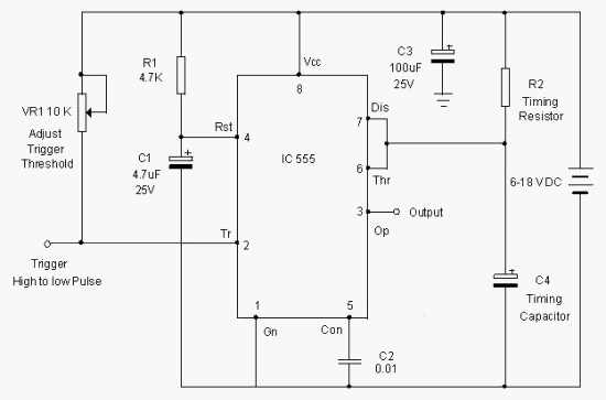
The circuit diagram shown below is the simple monostable using IC 555. To eliminate the false triggering resistor R1 and Capacitor C1 are connected to the reset pin 4 of the IC. So the reset pin is always high even if the supply voltage changes. Moreover capacitor C3 connected close to the Vcc pin 8 acts as a buffer to maintain stable supply voltage to pin 8. Using this design, it is easy to avoid false triggering to a certain extent.
555 Monostable circuit
A ready recknor to select timing resistor and capacitor
Theoretically long interval is possible with IC 555,but in practical conditions, it is difficult to get more than 3 minutes. If low leakage Tantalum capacitor is used, this can be increased to 5 minutes or more. If the value of the timing capacitor is too high above 470 uF, charging time will be prolonged which will upset the timing cycle and the output remains high even after the desired time is over.
TV Remote Jammer Using 555 IC Circuit Diagram
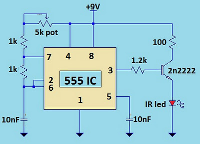
The TV remote control transmits television signals as pulses of frequency around 37.5kHz. Each button on the remote control is pressed or equivalent has a pulse signal codes. This remote transmits pulses of the circuit block of the same frequency as the remote to your TV confuse decoding the transmitted signal.
The heart of the circuit is the 555 timer IC in astable circuit works mode.The output series of pulses at a frequency of 18 kHz to 48 kHz by simply adjusting the 5K potentiometer. What you do is adjust the potentiometer until frequeny jives to its distance from the TV or until the signal is ignored by television.
TV Remote Jammer Using 555 IC Circuit Diagram
Simple Two 555 Timers Bell Circuit Diagram
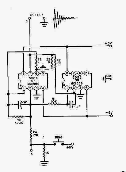
This is the Simple Two 555 Timers Bell Circuit Diagram. This simple scheme uses two Bell 555 timer. The frequency controlled capacitors, which should be preserved are almost identical in value with each other to achieve the best results. Fine tuning is done with the R1 and R2. The decay time is controlled by R3.
Simple Two 555 Timers Bell Circuit Diagram
simple Acoustic Sensor-Circuit Diagram
This acoustic sensor was originally developed for an industrial application (monitoring a siren), but will also find many domestic applications. Note that the sensor is designed with safety of operation as the top priority: this means that if it fails then in the worst-case scenario it will not itself generate a false indication that a sound is detected. Also, the sensor connections are protected against polarity reversal and short-circuits. The supply voltage of 24 V is suitable for industrial use, and the output of the sensor swings over the supply voltage range.
Circuit diagram :
The circuit consists of an electret micro-phone, an amplifier, attenuator, rectifier and a switching stage. MIC1 is supplied with a current of 1 mA by R9. T1 amplifies the signal, decoupled from the supply by C1, to about 1 Vpp. R7 sets the collector current of T1 to a maximum of 0.5 mA. The operating point is set by feedback resistor R8. The sensitivity of the circuit can be adjusted using potentiometer P1 so that it does not respond to ambient noise levels. Diodes D1 and D2 recitfy the signal and C4 provides smoothing. As soon as the voltage across C4 rises above 0.5 V, T2 turns on and the LED connected to the collector of the transistor lights. T3 inverts this signal.
If the microphone receives no sound, T3 turns on and the output will be at ground. If a signal is detected, T3 turns off and the output is pulled to +24 V by R4 and R5. In order to allow for an output current of 10 mA, T3’s collector resistor needs to be 2.4 kΩ. If 0.25 W resistors are to be used, then to be on the safe side this should be made up of two 4.7 kΩ resistors wired in parallel. Diode D4 protects the circuit from reverse polarity connection, and D3 protects the output from damage if it is inadvertently connected to the supply.
Water-Tank Level Meter Sensor
The water-tank level meter de-scribed here is very simple and useful for monitoring the water level in an overhead tank (OHT). The water level at 30cm intervals is monitored and continuously indicated by LEDs ar-ranged in a meter-format. When all the LEDs are ‘off’, it indicates that the OHT is empty. When the water level reaches the top limit, the whole LED-meter begins to flash. The height at which the level-sensing electrodes are fitted is adjustable. Thus, the minimum and maximum level settings may be varied as desired. The range of the meter can also be enlarged to cater to any level. No special or critical components are used. CMOS ICs are used to limit the idle current to a minimum level.
Even when all the LEDs are ‘on’, i.e. water reaches the top level, the demand on the power supply is reasonably low. Further, the extremely high input resistance of the Schmitt inverter gates reduces the input current and thus minimises the erosion of electrodes. The princi-pal part of the device is its water-level sensor assembly. By using easily available material, it can be fabricated to meet one’s own specific requirements. The common ground reference electrode ‘X’ is an aluminium conduit of 15mm outer diameter and 3-metre length, to cater to a 3-metre deep overhead tank. Insulating spacer rings ‘Y’ (10mm length, 15mm dia.) are fabricated from electrical wiring conduits of 15mm inner diameter.
These are pushed tightly over the aluminum conduit at preferred places, say 30cm apart. If the pieces are too tight, they can be heated in boiling water for softening and then pushed over ‘X’. The sensor electrodes ‘Z’ are made out of copper or brass strips (6mm wide and 1mm thick) which are shaped into rings that can tightly slip over the ‘Y’ pieces. The ends of these strips are folded firmly and formed into solder tags S1 to S10 and SG. The wall-mounting brackets, made of aluminium die-cast, are screwed directly on ‘X’ at two suitable places.
The sensor cable ‘WC’ wires are soldered to solder tags, and some epoxy cement is applied around the joints and tags to avoid corrosion by water. The common ground reference wire ‘SG’ is taken from tag ‘T’. T
e cable’s individual wires from S1 to S10 and SG are cut and matched in length for a neat layout. The other ends of the cable are connected to the PCB terminal points S1 to S10 and SG respectively. No separate ground is needed. The electronics portion is simple and straightforward. A long piece of vero board can hold all the parts including the power supply section.
For easy installation, the LEDs can be set at the track side of the board, in a single line, so that they may be pushed through the cutouts in the front panel of the enclosure from inside. The water level at 30cm intervals is monitored by corresponding sensors, causing the input to the concerned inverters (normally pulled ‘high’ via resistors R1 through R10) to go ‘low’, as soon as water reaches the respective sensors On initial switching ‘on’ of the power supply, when the tank is empty, all the electrodes are open. As a result, all the inverter inputs are ‘high’ (via the pull-up resistors R1 to R10) and their outputs are all ‘low’. Thus, all the LEDs are ‘off ’. As soon as the water starts filling the tank, the rising water level grounds the first sensor.
The logic 1 output of first inverter gate N1 causes conduction of transistor T2 to extend ground to one side of resistors R14 through R23 via emitter collector path of transistor T2. The LED D1 is thus lit up. Similarly, other LEDs turn ‘on’ successively as the water level rises. As soon as the water in OHT reaches the top level, the output of gate N10 goes to logic 1 and causes flashing-type LED D11 to start flashing. At the same time, transistor T1 conducts and cuts off alternately, in synchronism with LED D11’s flash rate, to ground the base of transistor T2 during conduction of transistor T1. As a result, transistor T2 also starts cutting ‘off’ during conduction of transistor T1, to make the LED meter (comprising LEDs D1 through D10) flash and thus warn that the water has reached the top level.
When the water level goes down, the reverse happens and each LED is turned ‘off’ successively. The novel feature of this circuit is that whenever the water level is below the first sensor, all the LEDs are ‘off’ and the quiescent current is very low. Thus, a power ‘on’/‘off’ switch is not so essential. Even when the LED-meter is fully on, the cur-rent drawn from the power supply is not more than 120 mA. A heat-sink may, how-ever, be used for transistor T2, if the tank is expected to remain full most of the time. A power supply unit providing unregulated 6V DC to 15V DC at 300mA current is adequate.
Caution. A point to be noted is that water tends to stick to the narrow space at the sensor-spacer junction and can cause a false reading on the LED-meter. This can be avoided if the spacers are made wider than 10 mm. Author : M.K. Chandra MouleeswAran - Copyright : EFY
LM35 Temperature Sensor Circuit Diagram
The LM35 temperature sensor provides an output of 10 mV/C for every degree Celsius over 0C. At 20C the output voltage is 20 10 = 200 mV. The circuit consumes 00.
LM35 Temperature Sensor Circuit Diagram
The load resistance should not be less than 5 kQ. A 4- to 20-V supply can be used.
LM35 Temperature Sensor Circuit Diagram
The load resistance should not be less than 5 kQ. A 4- to 20-V supply can be used.
Simple Temperature Sensor Circuit using 1N4148 diode
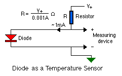
There are components that have special characteristics, one of them is the 1N4148 diode, it is a diode High-speed, and its switching speed is 4th, its voltage is 100 V and current of 450 mA. It besides a diode 1N4148 is used as the temperature sensor, that due to its characteristics that cause it to change its resistance with temperature change. Of course it does not compare to a sensor like the LM38, but for some circuits of low precision, which just need to know if an element is hot or cold it is very useful.
Using the multimeter and the 1N4148 as a thermometer
The scheme above is a circuit that measures the temperature in a simple manner using a multimeter. It uses 1N4148 diode, and VR1 and VR2 must be adjusted with a thermometer, and is more precise measurement. On the scale of the multimeter can be compared to the scale of degree Celsius with Volt.
Temperature sensor with diode 1N4148
Vibration sensors Circuit Diagram
The vibration sensors can be very useful in alarm systems and automation, but are usually a bit expensive. This sensor utilizes a piezo sounder elements to detect vi rations coming. The circuit uses reverse engineering and vibration sensor circuit that can be used in a toy dog that barks when he feels a vibration near the same on their projects using Arduino microcontrollers .
Here is a picture element piezo vibration sensor.
How to Using Diodes as a photosensor Circuit diagram
A photo diode is a PN junction or PIN structure that when light reaches the junction, it excites an electron thereby creating a free electron positively charged. This mechanism is also known as the photoelectric effect, common in transistors, diodes and ICs are made of semiconductors, and contain PN junctions. Almost all of the potentially active constituents are a photo diode and may be used as a photo sensor. The PN junction needs to be exposed to light, so to use a semiconductor diode as a light bulb must have a transparent glass, these diodes with these characteristics can be used to measure the light intensity.
Circuit diagram of a light intensity meter with diode.
a test circuit diode light sensor
List of components:
D1 1n148 or any other photo-sensitive element
T1, T2 BC548 or similar
C1 680n
R1 2M
Above this circuit that is very popular, it works with LEDs, photodiodes and photo-resistors. V is a voltmeter which can be a multimeter.
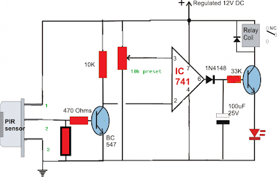
Build a Passive Infrared Sensor Circuit
What is PIR ?Passive Infrared Sensor Circuit Diagram. Detectors or pyroelectric sensors, passive infrared or PIR sensor, are made of a crystalline material that generates an electric charge on the surface when exposed to heat in the form of infrared radiation. When radiation increases the amount of electrical charge increases too and this load is measured with a sensitive FET transistor which is inside the sensor module.
With the RIP is commonly used as a motion detector of an object by detecting the infrared signal radiated from the object (people and animals). The Passive Infrared Sensors are also used in remote thermometers.
Pin 1 of the PIR must be connected to the positive supply 5V DC. Pin 2 is the output of PIR sensor, it must have a connection to the earth through a resistor of 47K to 100K (depending on the circuit). Pin 3 of the RIP must be connected to ground or negative circuit.
Simple Circuit Diagram using PIR Sensor
Simple circuit motion sensor PIR detector.
Connect the PIR sensor in Arduino
The image above shows a PIR sensor as a switch connected to an Arduino board using a 10k pull-down resistor.
Simple circuit motion sensor PIR detector.
Connect the PIR sensor in Arduino
The image above shows a PIR sensor as a switch connected to an Arduino board using a 10k pull-down resistor.
Room Noise Detector Schematic Circuit
This Room Noise Detector Schematic circuit diagram is intended to signal, through a flashing LED, the exceeding of a fixed threshold in room noise, chosen from three fixed levels, namely 50, 70 & 85 dB. Two Op-amps provide the necessary circuit gain for sounds picked-up by a miniature electret microphone to drive a LED. With SW1 in the first position the circuit is off. Second, third and fourth positions power the circuit and set the input sensitivity threshold to 85, 70 & 50 dB respectively. Current drawing is 1mA with LED off and 12-15mA when the LED is steady on.
Circuit diagram :
Room Noise Detector Circuit diagram
Parts List :
R1____________10K 1/4W Resistor
R2,R3_________22K 1/4W Resistors
R4___________100K 1/4W Resistor
R5,R9,R1
_____56K 1/4W Resistors
R6_____________5K6 1/4W Resistor
R7___________560R 1/4W Resistor
R8_____________2K2 1/4W Resistor
R11____________1K 1/4W Resistor
R12___________33K 1/4W Resistor
R13__________330R 1/4W Resistor
C1___________100nF 63V Polyester Capacitor
C2____________10µF 25V Electrolytic Capacitor
C3___________470µF 25V Electrolytic Capacitor
C4____________47µF 25V Electrolytic Capacitor
D1_____________5mm. Red LED
IC1__________LM358 Low Power Dual Op-amp
Q1___________BC327 45V 800mA PNP Transistor
MIC1_________Miniature electret microphone
SW1__________2 poles 4 ways rotary switch
B1___________9V PP3 Battery
Clip for PP3 Battery
Use :
- Place the small box containing the circuit in the room where you intend to measure ambient noise.
- The 50 dB setting is provided to monitor the noise in the bedroom at night. If the LED is steady on, or flashes bright often, then your bedroom is inadequate and too noisy for sleep.
- The 70 dB setting is for living-rooms. If this level is often exceeded during the day, your apartment is rather uncomfortable.
- If noise level is constantly over 85 dB, 8 hours a day, then you are living in a dangerous environment.
Tiny Dew Sensor Circuit Diagram
Tiny Dew Sensor Circuit Diagram (condensed moisture) adversely affects the normal performance of sensitive electronic devices. A low-cost circuit described here can be used to switch off any gadget automatically in case of excessive humidity. At the heart of the circuit is an inexpensive (resistor type) dew sensor element. Although dew sensor elements are widely used in video cassette players and recorders, these may not be easily available in local market. However, the same can be procured from authorized service cent res of reputed companies. The author used the dew sensor for FUNAI VCP model No. V.I.P. 3000A (Part No: 6808-08-04, reference no. 336) in his prototype.
In practice, it is observed that all dew sensors available for video application possess the same electrical characteristics irrespective of their physical shape/size, and hence are interchangeable and can be used in this project. The circuit is basically a switching type circuit made with the help of a popular dual op-amp IC LM358N which is configured here as a comparator. (Note that only one half of the IC is used here.) Under normal conditions, resistance of the dew sensor is low (1 kilo-ohm or so) and thus the voltage at its non-inverting terminal (pin 3) is low compared to that at its inverting input (pin 2) terminal.
Tiny Dew Sensor Cicuit Diagram Circuit Diagram:
The corresponding output of the comparator (at pin 1) is accordingly low and thus nothing happens in the circuit. When humidity exceeds 80 per cent, the sensor resistance increases rapidly. As a result, the non-inverting pin becomes more positive than the inverting pin. This pushes up the output of IC1 to a high level. As a consequence, the LED inside the opto-coupler is energized. At the same time LED1 provides a visual indication. The opto-coupler can be suitably interfaced to any electronic device for switching purpose. Circuit comprising diode D1, resistors R8 and R6 and capacitor C1 forms a low-voltage, low-current power supply unit. This simple arrangement obviates the requirement for a bulky and expensive step-down transformer.
In practice, it is observed that all dew sensors available for video application possess the same electrical characteristics irrespective of their physical shape/size, and hence are interchangeable and can be used in this project. The circuit is basically a switching type circuit made with the help of a popular dual op-amp IC LM358N which is configured here as a comparator. (Note that only one half of the IC is used here.) Under normal conditions, resistance of the dew sensor is low (1 kilo-ohm or so) and thus the voltage at its non-inverting terminal (pin 3) is low compared to that at its inverting input (pin 2) terminal.
Tiny Dew Sensor Cicuit Diagram Circuit Diagram:
Tiny Dew Sensor Circuit Diagram
The corresponding output of the comparator (at pin 1) is accordingly low and thus nothing happens in the circuit. When humidity exceeds 80 per cent, the sensor resistance increases rapidly. As a result, the non-inverting pin becomes more positive than the inverting pin. This pushes up the output of IC1 to a high level. As a consequence, the LED inside the opto-coupler is energized. At the same time LED1 provides a visual indication. The opto-coupler can be suitably interfaced to any electronic device for switching purpose. Circuit comprising diode D1, resistors R8 and R6 and capacitor C1 forms a low-voltage, low-current power supply unit. This simple arrangement obviates the requirement for a bulky and expensive step-down transformer.
Source:pecworld.zxq
Simple Park Assist Circuit Diagram
Build a Park Assist Circuit Diagram. This is a Simple Park Assist Circuit Diagram. This Park Assist circuit was designed as an aid in parking the car near the garage wall when backing up. LED D7 illuminates when bumper-wall distance is about 20 cm., D7+D6 illuminate at about 10 cm. and D7+D6+D5 at about 6 cm. In this manner you are alerted when approaching too close to the wall.
All distances mentioned before can vary, depending on infra-red transmitting and receiving LEDs used and are mostly affected by the color of the reflecting surface. Black surfaces
lower greatly the device sensitivity. Obviously, you can use this circuit in other applications like liquids level detection, proximity devices etc.
Simple Park Assist Circuit Diagram
Shutter Guard Circuit diagram
This Shutter Guard Circuit diagram sensitive vibration sensor is exclusively made for shops to protect against burglary. It will detect any mechanical or acoustic vibration in its vicinity when somebody tries to break the shutter and immediately switch on a lamp and sound a warning alarm. A 15-minute time delay after switch-on allows sufficient time for the shop owner to close the shutter.
Shutter Guard Circuit diagram :Shutter Guard Circuit Diagram
The front end of the circuit has a timer built around the popular binary counter IC CD4060 (IC1) to provide 15-minute time delay for the remaining circuitry to turn on. Resistors R3 and R4 and capacitor C2 will make Q9 output high after 15 minutes. Di-ode D1 inhibits the clock input (pin 11) to keep the output high till the power is switched off. Blinking LED1 indicate the oscillation of IC1.
The high output from IC1 is used to enable reset pin 4 of IC2 so that it can function freely. Transistor T1 amplifies the piezo-sensor signal and triggers monostable IC2. The base of transistor T1 is biased using a standard piezo element that acts as a small capacitor and flexes freely in response to mechanical vibrations so that the output of IC2 is high till the prefixed time period. In the standby mode, the alarm circuit built around IC3 remains dormant as it does not get current. Timing components R8 and C6 make the output of IC2 high for a period of three minutes.
When any mechanical vibration (caused by even a slight movement) disturbs the piezo element, trigger pin 2 of IC2 momentarily changes its state and the output of IC2 goes high. This triggers triac 1 and the alarm circuit activates. Triac BT136 completes the lamp circuit by activating its gate through resistor R9. IC UM3561 (IC4) generates a tone simulating the police siren with R11 as its oscillation-controlling resistor. Zener diode ZD1 provides stable 3.1V DC for the tone-generating IC.
Assemble the circuit on a general-purpose PCB and enclose in a suit-able, shockproof case. Connect the piezo element to the circuit by using a single-core shielded wire. Glue a circular rubber washer on the fine side of the piezo element and fix it on the shutter frame with the washer facing the frame so that the piezo element is flexible to sense the vibrations. Fix the lamp and the speaker on the outer side and the remaining parts inside the case. Since triac is used in the circuit, most points in the PCB will be at mains lethal potential. So it is advised not to touch any part of the circuit while testing.
Fog Lamp Sensor-Circuit Diagram
Fog Lamp Sensor Circuit diagram . For several years now, a rear fog lamp has been mandatory for trailers and caravans in order to improve visibility under foggy conditions.
Fog Lamp Sensor Circuit diagram :
Fog Lamp Sensor Circuit Diagram
When this fog lampis switched on, the fog lamp of the pulling vehicle must be switched off to avoid irritating reflections. For this purpose, a mechanical switch is now built into the 13-way female connector in order to switch off the fog lamp of the pulling vehicle and switch on the fog lamp of the trailer or caravan. For anyone who uses a 7-way connector, this switching can also be implemented electronically with the aid of the circuit illustrated here. Here a type P521 opto coupler detects whether the fog lamp of the caravan or trailer is connected. If the fog lamp is switched on in the car, a current flows through the caravan fog lamp via diodes D1 and D2. This causes the LED in the opto coupler to light up, with the result that the phot otransistor conducts and energises the relay via transistor T1. The relay switches off the fog lamp of the car.
For anyone who’s not all thumbs, this small circuit can easily be built on a small piece of perforated circuit board and then fitted somewhere close to the rear lamp fitting of the pulling vehicle.
Colour Sensor Circuit
Colour Sensor Circuit diagram is an interesting project for hobbyists. The circuit can sense eight colours, i.e. blue,green and red (primary colours); magenta, yellow and cyan (secondary colours); and black and white. The circuit is based on the fundamentals of optics and digital electronics.
Colour Sensor Circuit diagram :
Colour Sensor Circuit Diagram
The object whose colour is required to be detected should be placed in front of the system. The light rays reflected from the object will fall on the three convex lenses which are fixed in front of the three LDRs. The convex lenses are used to converge light rays. This helps to increase the sensitivity of LDRs. Blue, green and red glass plates (filters) are fixed in front of LDR1, LDR2 and LDR3 respecti ely. When reflected light rays from the object fall on the gadget, the coloured filter glass plates determine which of the LDRs would get triggered. The circuit makes use of only ‘AND’ gates and ‘NOT’ gates. When a primary coloured light ray falls on the system, the glass plate corresponding to that primary colour will allow that specific light to pass through. But the other two glass plates will not allow any light to pass through. Thus only one LDR will get triggered and the gate output corresponding to that LDR will become logic 1 to indicate which colour it is. Similarly, when a secondary coloured light ray falls on the system, the two primary glass plates corresponding to the mixed colour will allow that light to pass through while the remaining one will not allow any light ray to pass through it. As a result two of the LDRs get triggered and the gate output corresponding to these will become logic 1 and indicate which colour it is.
When all the LDRs get triggered or remain untriggered, you will observe white and black light indications respectively. Following points may be carefully noted:
- 1. Potmeters VR1, VR2 and VR3 may be used to adjust the sensitivity of the LDRs.
2. Common ends of the LDRs should be connected to positive supply.
3. Use good quality light filters.
The LDR is mounded in a tube, behind a lens, and aimed at the object. The coloured glass filter should be fixed in front of the LDR as shown in the figure. Make three of that kind and fix them in a suitable case. Adjustments are critical and the gadget performance would depend upon its proper fabrication and use of correct filters as well as light conditions.
Tester for Inductive Sensors
This tester uses a LED to indicate whether an inductive sensor is generating a signal. It can be used to test the inductive sensors used in ABS and EBS systems in cars, with engine cam- shafts and flywheels, and so on. The circuit is built around an LM358 dual opamp IC. The weak signal coming from the sensor (when the wheel is turning slowly, for example) is an AC voltage. The first opamp, which is wired here as an inverting amplifier, amplifies the negative half cycles of this signal by a factor of 820. The second opamp is wired as a comparator and causes the red LED to blink regularly.
In order to judge the quality of the signal from the sensor, you must turn the wheel very slowly. If the red LED blinks, this means that the sensor is generating a signal and the distance between the sensor and the pole wheel (gear wheel) is set correctly. If the distance (air gap) is too large, the sensor will not generate a signal when the wheel is turned slowly, with the result that the LED will remain dark, but it will generate a signal if the wheel is turned faster and the LED will thus start blinking. Irregularities in the blinking rate can be caused by dirt on the sensor or damage to the pole wheel (gear wheel). Tester for Inductive Sensors Circuit diagram:
In order to judge the quality of the signal from the sensor, you must turn the wheel very slowly. If the red LED blinks, this means that the sensor is generating a signal and the distance between the sensor and the pole wheel (gear wheel) is set correctly. If the distance (air gap) is too large, the sensor will not generate a signal when the wheel is turned slowly, with the result that the LED will remain dark, but it will generate a signal if the wheel is turned faster and the LED will thus start blinking. Irregularities in the blinking rate can be caused by dirt on the sensor or damage to the pole wheel (gear wheel).
Tester for Inductive Sensors Circuit DiagramIf you connect an oscilloscope to the LED with the engine running, you will see a square-wave signal with a pattern matching the teeth of the gear wheel, with a frequency equal to the frequency of the AC signal generated by the sensor. You can also use this tester to check the polarity of the connecting leads. To do this, first dismount the sensor and then move it away from a metal-lic object. The LED will go on or off while the sensor is moving. If you now reverse the lead connections, the LED should do exactly the opposite as before when the sensor is moved the same way.
The circuit has been tested extensively in several workshops on various vehicles, and it works faultlessly. The author has also connected the tester to sensors on running engines, such as the cam-shaft and flywheel sensors of a Volvo truck (D13 A engine). With the camshaft sensor, the LED blinks when the engine is being cranked for starting, but once the engine starts running you can’t see the LED blinking any more due to the high blinking rate.
Simple Temperature Sensor + Arduino
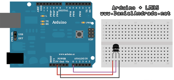
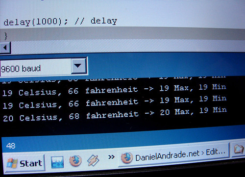
Today I am going to show you how to build a simple temperature sensor using one LM35 Precision Temperature Sensor and Arduino, so you can hookup on your future projects. The circuit will send serial information about the temperature so you can use on your computer, change the code as you will. I’m planning to build a temperature sensor with max/min + clock + LCD, and when I get it done, I will post here.
Parts:
- Arduino (You can use other microcontroller, but then you will need to change the code).
- LM35 Precision Centigrade Temperature Sensor, you can get from any electronic store. Here is the DATA SHEET.
- BreadBoard
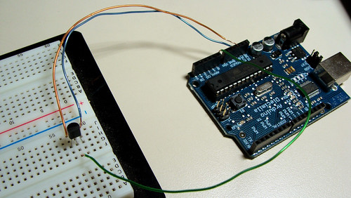
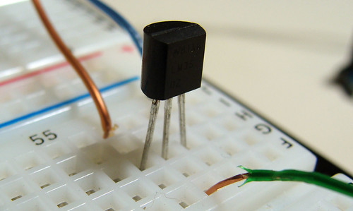
This is a quick and simple step. Just connect the 5V output from arduino to the 1st pin of the sensor, ground the 3rd pin and the 2nd one, you connect to the 0 Analog Input.
Down goes some pictures that may help you, click to enlarge:
Here is the Arduino Code, just upload it and check the Serial Communication Option.
You can also download the .pde HERE.
/*
An open-source LM35DZ Temperature Sensor for Arduino. This project will be
enhanced on a regular basis
(cc) by Daniel Spillere Andrade , http://www.danielandrade.net
http://creativecommons.org/license/cc-gpl
*/
int pin = 0; // analog pin
int tempc = 0,tempf=0; // temperature variables
int samples[8]; // variables to make a better precision
int maxi = -100,mini = 100; // to start max/min temperature
int i;
void setup()
{
Serial.begin(9600); // start serial communication
}
void loop()
for(i = 0;i< =7;i++){ // gets 8 samples of temperature
samples[i] = ( 5.0 * analogRead(pin) * 100.0) / 1024.0;
tempc = tempc + samples[i];
delay(1000);
}
tempc = tempc/8.0; // better precision
tempf = (tempc * 9)/ 5 + 32; // converts to fahrenheit
if(tempc > maxi) {maxi = tempc;} // set max temperature
if(tempc < mini) {mini = tempc;} // set min temperature
Serial.print(tempc,DEC);
Serial.print(" Celsius, ");
Serial.print(tempf,DEC);
Serial.print(" fahrenheit -> ");
Serial.print(maxi,DEC);
Serial.print(" Max, ");
Serial.print(mini,DEC);
Serial.println(" Min");
tempc = 0;
delay(1000); // delay before loop
}
Anything just ask!
Sensor and Detector Liquids Circuit
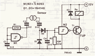
This is a very simple liquid detector which controls a relay, this gives you the option to be used for hundreds of applications. You can use it as a float switch to turn on the water pump alarm, rain, etc.. He uses a 4093 IC and transistor can be anyone, provided that it meets the power relay. This sensorcan be used with Arduino no problem .
Sensor and Detector Liquids Circuit Diagram
Line Following Robot Sensor
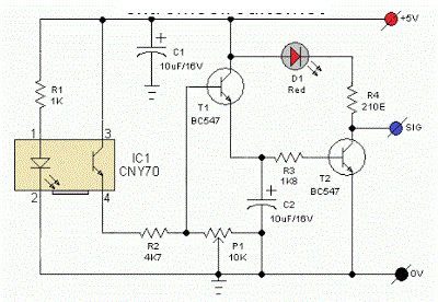
This Line Following Robot sensor or surface scanner for robots is a very simple, stamp-sized, short range (5-10mm) Infrared proximity detector wired around a standard reflective opto-sensor CNY70(IC1). In some disciplines, a line following robot or an electronic toy vehicle go along a pre drawn black line on a white surface. In such devices, a surface scanner, pointed at the surface is used to align the right track.
IC1 contains an infrared LED and a photo transistor. The LED emit invisible infrared light on the track and the photo transistor works as a receiver. Usually, black colored surface reflects less light than white surface and more current will flow through the photo transistor when it is above a white surface. When a reflection is detected (IR light falls on the photo transistor) a current flows through R2 to ground which generates a voltage drop at the base of T1 to make it conduct. As a result, transistor T2 start conducting and the visual indicator LED(D1) lights up. Capacitor C2 works as a mini buffer.
Line Follower Robot Scanner Schematic
After construction and installation, the scanner needs to be calibrated. Initially set P1 to its mechanical centre position and place the robot above the white portion of the track. Now slowly turn P1 to get a good response from D1. After this, fine tune P1 to reduce false detection caused by external light sources. Also ensure that the LED remains in off condition when the sensor module is on the blackarea. Repeat the process until the correct calibration is achieved.
The red color LED (D1) is only a visual indicator. You can add a suitable (5V) reed relay in parallel with D1-R4 wiring after suitable alterations to brake/stop/redirect the robot. Similarly, the High to low (H-L) transition at the collector of T2 can be used as a signal to control the logic blocks of the robot. Resistor R1 determines the operating current of the IRLED inside IC1. The sensing ability largely depends on the reflective properties of the markings on the track and the strength of the light output from IC1.
Simple Relay Output Proximity Sensor Circuit
This is the Simple Relay Output Proximity Sensor Circuit Diagram. In This Circuit Ql is used as an oscillator around 300 kHz. R9 is set so that the oscillator just begins to run. An object ne ar the antenna will load the circuit down, and stop the oscillations. This is detected by buffer Q2, diodes Dl and D2, and this activates relay driver Q4, which operates the relay.
Simple Relay Output Proximity Sensor Circuit Diagram
Simple Dual Trace Scope Switch Circuit
Simple Dual Trace Scope Switch Circuit Diagram. The switcher output goes to the single vertical input of the scope, and a sync line from one of the inputs is taken to the scope's external-sync input. Frequency response of the input amplifiers is 300 kHz over the range of the gain controls. With the gain controls wide open so no attenuation of the signal takes place, the frequency response is up to 1 MHz.
Simple Comparator with time out Circuit Diagram
This is a Simple Comparator with time out Circuit Diagram. The MC1422 is used as a comparator with input (Pin 5). The frequency of the pulses for the capability of a timing output pulse when the the values of R2 and Cl as shown is approx i-inverting input (Pin 6) is the non inverting mately 2 Hz, and the pulse width 0 ms.
Simple Comparator with time out Circuit Diagram
Simple Voltage to Current Converter Circuit
This is a Simple Voltage to Current Converter Circuit Diagram. This is an electronic circuit, The current out is Iqut—Vin/R. For negative currents, a PNP can be used and, for better accuracy,-a Darlington pair can be substituted for the transistor. With careful design, this circuit can be used to control currents of many amps Unity gain compensation is necessary.
Simple Voltage to Current Converter Circuit Diagram
Frequency to voltage converter using LM331
LM331 is basically a precision voltage to frequency converter from National Semiconductors. The IC has a hand full of applications like analog to digital conversion, long term integration, voltage to frequency conversion, frequency to voltage conversion. Wide dynamic range and excellent linearity makes the IC well suitable for the applications mentioned above.
Here the LM331 is wired as a frequency to voltage converter which converts the input frequency into a proportional voltage which is extremely linear to the input frequency. The frequency to voltage conversion is attained by differentiating the input frequency using capacitor C3 and resistor R7 and feeding the resultant pulse train to the pin6 (threshold) of the IC. The negative going edge of the resultant pulse train at pin6 makes the built-in comparator circuit to trigger the timer circuit. At any instant, the current flowing out of the current output pin (pin 6) will be proportional to the input frequency and value of the timing components (R1 and C1). As a result a voltage (Vout) proportional to the input frequency (Fin) will be available across the load resistor R4.
Notes.
Here the LM331 is wired as a frequency to voltage converter which converts the input frequency into a proportional voltage which is extremely linear to the input frequency. The frequency to voltage conversion is attained by differentiating the input frequency using capacitor C3 and resistor R7 and feeding the resultant pulse train to the pin6 (threshold) of the IC. The negative going edge of the resultant pulse train at pin6 makes the built-in comparator circuit to trigger the timer circuit. At any instant, the current flowing out of the current output pin (pin 6) will be proportional to the input frequency and value of the timing components (R1 and C1). As a result a voltage (Vout) proportional to the input frequency (Fin) will be available across the load resistor R4.
Circuit diagram.
Notes.
- The circuit can be assembled on a vero board.
- I used 15V DC as the supply voltage (+Vs) while testing the circuit.
- The LM331 can be operated from anything between 5 to 30V DC.
- The value of R3 depends on the supply voltage and the equation is R3= (Vs – 2V)/ (2mA).
- According to the equation, for Vs = 15V, R3=68K.
- The output voltage depends on the equation, Vout = ((R4)/(R5+R6))*R1C1*2.09V*Fin.
- POT R6 can be used for calibrating the circuit.
Battery charger circuit using L200
A very simple battery charger circuit having reverse polarity indication is shown here.The circuit is based on IC L200 . L200 is a five pin variable voltage voltage regulator IC. The charging circuit can be fed by the DC voltage from a bridge rectifier or center tapped rectifier.Here the IC L200 keeps the charging voltage constant.The charging current is controlled by the parallel combination of the resistors R2 & R3.The POT P1 can be used to adjust the charging current.
Battery charger circuit using L200 With Parts listThis circuit is designed to charge a 12 V lead acid battery.The transistor t1,diode D3 and LED are used to make a battery reverse indicator.In case the battery is connected in reverse polarity ,the reverse polarity indicator red LED D5 glows.When the charging process is going on the battery charging indicator green LED D4 glows.
Notes.
The circuit can be assembled on a good quality PCB or common board.
The values of R2 & R3 can be obtained from the equation,
(R2//R3) =( V5-2)/(Io).
Where V5 is the charging voltage (voltage at pin 5) and Io is the charging current.
The POT R8 can be used for fine adjustments of charging current.
If battery is connected in reverse polarity the RED LED will glow.
When the charging is going on the GREEN LED will glow. The rectified input voltage to the charger can be 18V.
Sourced By : Circuitstoday
Simple Lithium Ion Charger 2 Cell Circuit
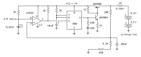
The below circuit is a Simple Lithium Ion Charger 2 Cell Circuit Diagram. This circuit was build to charge a couple series Lithium cells (3.6 volts each, 1 Amp Hour capacity) installed in a portable transistor radio.
The charger operates by supplying a short current pulse through a series resistor and then monitoring the battery voltage to determine if another pulse is required. The current can be adjusted by changing the series resistor or adjusting the input voltage. When the battery is low, the current pulses are spaced close together so that a somewhat constant current is present. As the batteries reach full charge, the pulses are spaced farther apart and the full charge condition is indicated by the LED blinking at a slower rate.
Simple Lithium Ion Charger 2 Cell Circuit Diagram
A TL431, band gap voltage reference (2.5 volts) is used on pin 6 of the comparator so that the comparator output will switch low, triggering the 555 timer when the voltage at pin 7 is less than 2.5 volts. The 555 output turns on the 2 transistors and the batteries charge for about 30 milliseconds. When the charge pulse ends, the battery voltage is measured and divided down by the combination 20K, 8.2K and 620 ohm resistors so that when the battery voltage reaches 8.2 volts, the input at pin 7 of the comparator will rise slightly above 2.5 volts and the circuit will stop charging.
The circuit could be used to charge other types of batteries such as Ni-Cad, NiMh or lead acid, but the shut-off voltage will need to be adjusted by changing the 8.2K and 620 ohm resistors so that the input to the comparator remains at 2.5 volts when the terminal battery voltage is reached.
For example, to charge a 6 volt lead acid battery to a limit of 7 volts, the current through the 20K resistor will be (7-2.5)/ 20K = 225 microamps. This means the combination of the other 2 resistors (8.2K and 620) must be R=E/I = 2.5/ 225 uA = 11,111 ohms. But this is not a standard value, so you could use a 10K in series with a 1.1K, or some other values that total 11.11K
Be careful not to overcharge the batteries. I would recommend using a large capacitor in place of the battery to test the circuit and verify it shuts off at the correct voltage.
100Khz Multiple Output Switching Power Supply Circuit
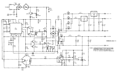
The 100Khz Multiple Output Switching Power Supply Circuit Diagram uses two VN4000A 400-V MOS POWER FETs in a half-bridge power switch configuration. Outputs available are + 5 Vat 20 A and ±15 V (or ±12 V) at 1 A. Since linear three-terminal regulators are used for the low-current outputs, either ±12 V or ±15 V can be made available with a simple change in the transformer secondary windings.
A TU94 switching regulator IC pro Vides pulse-width modulation control and drive signals for the power supply. The upper MOS POWER FET, Q7. in the power switch stage is driven by a simple transformer drive circuit. The lower MOS. Q6, since it is ground referenced. is directly driven from the control !C.
100Khz Multiple Output Switching Power Supply Circuit Diagram
Infrared Proximity Detector Circuit
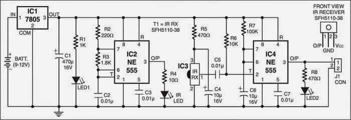
This proximity detector using an infrared detector (Fig. 1) can be used in various equipment like automatic door openers and burglar alarms. The circuit primarily consists of an infrared transmitter and an infrared receiver.
Fig. 1: IR proximity detector
The transmitter section consists of a 555 timer IC functioning in astable mode. It is wired as shown in the figure. The output from astable is fed to an infrared LED via resistor R4, which limits its operating current. This circuit provides a frequency output of 38 kHz at 50 per cent duty cycle, which is required for the infrared detector/receiver module. Siemens SFH5110-38 is a much better choice than SFH506-38. Siemens SFH5110-38 is turned on by a continuous frequency of 38 kHz with 50 per cent duty cycle, whereas SFH506 requires a burst frequency of 38k to sense. Hence, SFH5110-38 is used.The receiver section comprises an infrared receiver module, a 555 monostable multivibrator, and an LED indicator. Upon reception of infrared signals, 555 timer (mono) turns on and remains on as long as infrared signals are received. When the signals are interrupted, the mono goes off after a few seconds (period=1.1 R7xC6) depending upon the value of R7-C6 combination. Thus if R7=470 kilo-ohms and C6=4.7µF, the mono period will be around 2.5 seconds.
Fig. 2: Proposed arrangement for separation of IR LED and receiver module in the proximity detector
Both the transmitter and the receiver parts can be mounted on a single breadboard or PCB. The infrared receiver must be placed behind the infrared LED to avoid false indication due to infrared leakage.
An object moving nearby actually reflects the infrared rays emitted by the infrared LED. The infrared receiver has sensitivity angle (lobe) of 0-60 degrees, hence when the reflected IR ray is sensed, the mono in the receiver part is triggered. The output from the mono may be used in any desired fashion. For example, it can be used to turn on a light when a person comes nearby by energising a relay. The light would automatically turn off after some time as the person moves away and the mono pulse period is over.
The sensitivity of the detector depends on current-limiting resistor R4 in series with the infrared LED. Range is approximately 40 cm. For 20-ohm value of R4 the object at 25 cm can be sensed, while for 30-ohm value of R4 the sensing range reduces by 22.5 cm.
(Note. The author procured the samples of Siemens products from Arihant Electricals, New Delhi, the distributor of Siemens in India.)
This circuit costs around Rs 125.
Sourced By: EFY Author : K.S. Sankar
Sawtooth to Triangle Converter for Oscillator Circuit
This wave shaper needs an input saw that goes from Vss to (ideally) Vdd. It works well with the 4069 VCO designed by René Schmitz. Any saw will work as long as the wave is centered halfway between the rails. It works as follows: The upper set of 2 linear mode gates provide an inverted and noninverted copy of the saw. The 3 logic gates at the bottom provide a sort of comparator that switches at halfway between the rails.
Sawtooth to Triangle Converter for Oscillator Circuit Diagram
The 4007 provides 2 P-MOSFETs that alternately select the inverted or noninverted saw signal depending on where the saw is in it's cycle. This causes the ramp to reverse directions every half cycle. Any imperfection in the saw will show up in the resulting output. The linear mode gate furthest to the right provides soft clipping that turns the triangle wave into something like a sine wave. It sounds like it has fewer harmonics than the triangle. To use with FatMan sawtooth output:
Power all ICs: Vdd = 0 volts, Vss = -12 volts. All ground symbols on schematic will go to -12 volts and all +V symbols go to ground.
Designed by René Schmitz
Simple Portable Solar Lantern Circuit
This is the Simple Portable Solar Lantern Circuit Diagram. This portable solar lantern circuit uses 6 volt/5 watt solar panels are now widely available. With the help of such a photo-voltaic panel we can construct an economical, simple but efficient and truly portable solar lantern unit. Next important component required is a high power (1watt) white LED module.
Simple Portable Solar Lantern Circuit Diagram
When solar panel is well exposed to sunlight, about 9 volt dc available from the panel can be used to recharge a 4.8 volt /600 mAh rated Ni-Cd batterypack. Here red LED (D2) functions as a charging process indicator with the help of resistor R1. Resistor R2 regulates the charging current flow to near 150mA.
Assuming a 4-5 hour sunlit day, the solar panel (150mA current set by the charge controller resistor R2) will pump about 600 – 750 mAh into the battery pack. When power switch S1 is turned on, dc supply from the Ni-Cd battery pack is extended to the white LED (D3). Resistor R3 determines the LED current. Capacitor C1 works as a buffer.
Note: After construction, slightly change the values of R1,R2 and R3 up/down by trial&error method, if necessary.
Controller of Solar charger Circuit
This is the simple Controller of Solar charger Circuit Diagram .When connecting a solar panel to a rechargeable battery, it is usually necessary to use a charge controller circuit to prevent the battery from overcharging. Charge control can be performed with a number of different circuit types. Lower power solar systems can use a series analog charge controller. Series regulators control the charging current by interrupting the flow of current from the solar panel to the battery when the battery reaches a preset full voltage. MPPT controllers use an inductor for energy storage and a high frequency switching circuit to transfer the energy to the battery.
This circuit is for a shunt-mode charge controller. In a shunt-mode circuit, the solar panel is permanently connected to the battery via a series diode. When the solar panel charges the battery up to the desired full voltage, the shunt circuit connects a resistive load across the battery to absorb the excess power from the solar panel. The main advantage of shunt-mode solar regulation is the lack of a switching transistor in the power path between the solar panel and battery. Switching transistors are non-perfect devices, they waste a percentage of available solar power as heat. Inefficiency in the shunt-mode controller’s switching transistor does not effect charging efficiency, it only turns on when excess power is purposely being wasted.
Solar power is routed from the PV panel through the 1N5818 Schottky diode to the battery. When the battery reaches the full setpoint, the output on the lower half of the TLC2272 dual op-amp turns on. This activates the IRFD110 MOSFET transistor and connects the 68 ohm 3W load resistor to the battery. The load across the battery causes the battery voltage to drop, and the comparator circuit turns back off. This oscillation continues while solar power is available. The 300nF capacitor across the op-amp slows the oscillation frequency down to a few hertz. The two 100K resistors in series provide a regulated 4.5V reference point for use as comparator reference points.
The 2N3906 transistor is wired with a zener diode in its base circuit, when the PV voltage is above 12V, the 2N3906 transistor turns on and enables the comparator circuit. The upper half of the TLC2272 op-amp inverts the dump load control signal, this is used to power the high intensity red LED. The LED turns on when the battery reaches the full setpoint. The LED does not waste any useful charging power since it only turns on when the battery is full.
The 78L09 IC provides 9V regulated power to the comparator circuitry. Operational power for this circuit is provided entirely from the PV panel, there is virtually no power taken from the battery at night.
This circuit can be modified for higher amperage by replacing the 1N5818 diode, 68 ohm load resistor and IRFD110 MOSFET with higher power components. If the load resistor is connected directly across the PV panel at noon on a sunny day, the PV output voltage should drop to 12V or less. Higher power PV panels will require a resistor with lower ohms and a higher wattage rating. In cold climates, it may be useful to use the load resistor’s heat to keep the battery warm.
Operation of a high power version of this circuit with a wind generator should be possible, although the author has not tried this. For a 20 amp version of this circuit, the IRFD110 MOSFET should be replaced with an IRFZ44N and the 1N5818 schottky diode should be replaced with a 20L15T. Both of these parts should have large heat sinks. The 68 ohm/3W resistor should be changed to a much larger resistor, An 0.6 ohm/250W resistor would be able to handle 20 amps at 12V.
This circuit is for a shunt-mode charge controller. In a shunt-mode circuit, the solar panel is permanently connected to the battery via a series diode. When the solar panel charges the battery up to the desired full voltage, the shunt circuit connects a resistive load across the battery to absorb the excess power from the solar panel. The main advantage of shunt-mode solar regulation is the lack of a switching transistor in the power path between the solar panel and battery. Switching transistors are non-perfect devices, they waste a percentage of available solar power as heat. Inefficiency in the shunt-mode controller’s switching transistor does not effect charging efficiency, it only turns on when excess power is purposely being wasted.
Controller of Solar charger Circuit Diagram
Solar power is routed from the PV panel through the 1N5818 Schottky diode to the battery. When the battery reaches the full setpoint, the output on the lower half of the TLC2272 dual op-amp turns on. This activates the IRFD110 MOSFET transistor and connects the 68 ohm 3W load resistor to the battery. The load across the battery causes the battery voltage to drop, and the comparator circuit turns back off. This oscillation continues while solar power is available. The 300nF capacitor across the op-amp slows the oscillation frequency down to a few hertz. The two 100K resistors in series provide a regulated 4.5V reference point for use as comparator reference points.
The 2N3906 transistor is wired with a zener diode in its base circuit, when the PV voltage is above 12V, the 2N3906 transistor turns on and enables the comparator circuit. The upper half of the TLC2272 op-amp inverts the dump load control signal, this is used to power the high intensity red LED. The LED turns on when the battery reaches the full setpoint. The LED does not waste any useful charging power since it only turns on when the battery is full.
The 78L09 IC provides 9V regulated power to the comparator circuitry. Operational power for this circuit is provided entirely from the PV panel, there is virtually no power taken from the battery at night.
This circuit can be modified for higher amperage by replacing the 1N5818 diode, 68 ohm load resistor and IRFD110 MOSFET with higher power components. If the load resistor is connected directly across the PV panel at noon on a sunny day, the PV output voltage should drop to 12V or less. Higher power PV panels will require a resistor with lower ohms and a higher wattage rating. In cold climates, it may be useful to use the load resistor’s heat to keep the battery warm.
Operation of a high power version of this circuit with a wind generator should be possible, although the author has not tried this. For a 20 amp version of this circuit, the IRFD110 MOSFET should be replaced with an IRFZ44N and the 1N5818 schottky diode should be replaced with a 20L15T. Both of these parts should have large heat sinks. The 68 ohm/3W resistor should be changed to a much larger resistor, An 0.6 ohm/250W resistor would be able to handle 20 amps at 12V.
Subscribe to:
Posts (Atom)