skip to main |
skip to sidebar
The explained crossover network is designed for applications where an original audio system is required to be used with a sub woofer speaker system.
This could be any sub woofer idling in your store room.
If the frequency specs of the loudspeaker are rated far down the spectrum then its better, nevertheless filter becomes always a handy option for the same in much effective way.
Usually a sub woofer circuit is in the form of an active filter, but with the botheration of having a separate power supply for powering the circuit.
The proposed sub woofer crossover network is a passive type by nature which allows the audio signal itself to get filtered through the associated passive components arranged in a calculated configuration.
Owing to the fact that the low frequency bass signal may be equally present in both the channels of the stereo signals, any of the channels may be used as the input source for feeding the sub woofer filter through an appropriate amplifier stage.
The shown design is a 1st order low pass filter consisting of a variable input option via pot P1 and also an adjustable cut off frequency preset P2.
The network comprising R1, R2, P1 is selected to be compatible with a 50 watt amplifier while the crossover frequency could be set anywhere from 50 Hz to 160 Hz using the preset P2.
The components R3, P2, C1 are configured assuming that the sub woofer amplifier which may be hooked up with K1 is compatible with an input resistance of 47k.
The diagram shows a relatively lower value for C1 which may be appropriately increased as per individual preferences.
For optimal performance it would be better to first keep the sub woofer amplifier volume fully open and get the sound level adjusted with the aid of P1.
This will make sure that the sub woofer amplifier never gets over loaded and stays safeguarded even with the highest sound pressures.
If the above consideration becomes unfeasible to be implemented an external overload protector may be used for the same.
In case a reversal of phase becomes essential, it may be suitably executed by swapping the wires which connects the sub woofer speaker
The circuit employs two strings of series connected lamps. One string is complimentary to the other, this means that when one string fades the other string gains luminescence. Two power transistors 2N3053 are connected in complimentary mode as shown in circuit 1. The collector of the first transistor is connected to base of the second one through a 2.2K resistor.
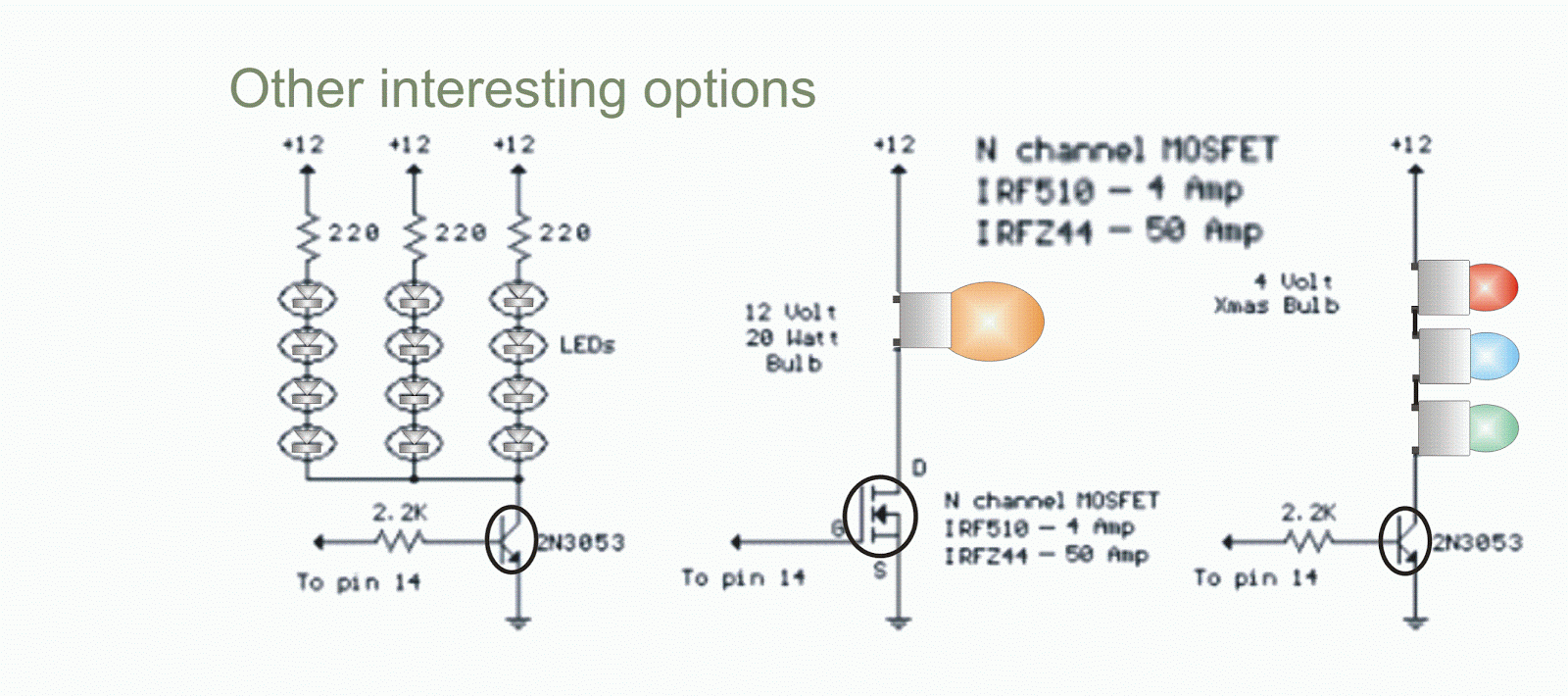
Different type of light source can be used by calculating the line current and bias voltages. Christmas tree bulb is a good option, as this bulb takes 200mA at 4V DC.
Three numbers in series thus do not require any current limiting resistance when applied voltage is 12V DC, as shown in the circuit. 2N3053 can smartly handle up to 500mA of current and hence using the same transistor three strings of LEDs can be connected in parallel with a current limiting resistance of 220ohm, as shown in circuit 2.
Four LEDs will be connected in a string, each LED chain will draw around 20mA of current. Hence, in practice, using the same transistor it is possible to connect nearly 12 to 15 strings in parallel that would draw a current of 240 to 300mA.
The principle of fading is designed around a quad OP-AMP LM324. One section of the IC is being used as a ramp generator, whereas the other section is used as a Schmitt trigger oscillator, for pleasure of vision the frequency of the ramp has been kept at 75Hz. In fact, the ramp circuit is the mother of all modern Pulse Width Modulation (PWM) circuit.
When a ramp is compared with a varying DC level, the output is pulse width modulating. This is conceived through simple geometry.
The frequency of the ramp is determined by the capacitor connected as shown by changing the values of the capacitor, the ramp frequency can be adjusted.
Instead of a NPN power transistor a MOSFET like IRZ44N is a good option. Such N channel MOSFETs are very smart and with a very nominal heat sink can handle much higher current than the NPN transistors.
This particular MOSFET is designed for a line current of 44 to 50 Amp depending on the junction temperature.
However, with proper heat sinks if the temperature rise is well monitored then such MOSFETs can smartly handle the current of 10- 15 Amp without any failure. While using MOSFET it is advisable to remember the power supply to the system should not go below 10V DC, as MOSFETs need a gate drive of 10V. 
It is sometimes disturbing to have a AM radio in a countryside and not being able to get the reception clearly. It is simply because of the distance of the radio station and also the strength of the station. The only solution is to attach a powerful antenna to the receiving radio the uniqueness of the antenna lies in its simplicity and cost. The basic knowledge of making an antenna is there in the back end.
Generally, the frequency range of amplitude modulation in 560 to 1650 KHz in order to resonate the LC circuit that that is the antenna (2πfL=1/(2πf_c ))
4πf^2 LC=1.Using this formula and using a 30- 450 pF gang condenser the handy inductance built on a 350ft long PVC pipe works quite well.
The inductance built around a PVC pipe is basically an air core inductor, the inductance of which is govern by the formula L=(R^2 N^2)/(9R+10l) where L is inductance in μH, R is coil radius in inches, l is coil length in inches and N is number of turns. The calculated inductance in tune with 33 pF- 330pF tuning capacitor should be around 250uH. Honestly with the proper geometrical calculation of winding a 3ft long PVC pipe an inductance value of 170uH is expected but in practice the inductance came out to be 213μH because of winding and error in winding spacing. The number of turn was around 500 and standard wire gauge of the wire 24. A secondary coil having 50 turns on the top of the primary was connected to the 4 turns of wire wound directly in the radio itself. His is to be noted that orientation should be such that the internal antenna of the radio should be co-axial with the external winding. Instead of this if you are allowed to open the radio set a few turns of the external antenna needs to be wound on the rod antenna of the radio. The best result is achieved when this tailored antenna is in perpendicular direction to the radio station and to be kept horizontal to the ground. The methodology of tuning the antenna is quite interesting. Firstly we need to select a very weak station of the AM band co that you hear sufficient amount of noise, at this point of time it is advisable to tune the gang condenser (antenna capacitor). Finally slight amount of physical adjustment of the rod maybe helpful. The electronic appliances, those have TRIACs , high voltage transformer, SMPs, high frequency devices may create electrical interferences and that is a concern, the antenna should be kept away from them.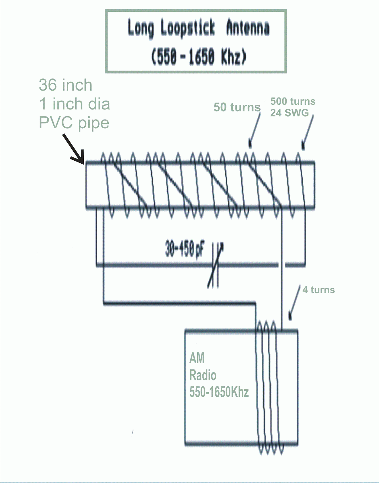
For a hobbyist, it has always been fun to activate or automate through a clap or a whistle. A whistle sometimes can act like a voice recognition actuator as the frequency varies from person to person. However, for this use the tuning is to be done around 1700 Hz, a pitch that is somewhere near to the middle C octave of the piano chords. A condenser microphone acts as the audio sensor and produces a few milli - volts of current to activate the electrical actuator like a relay. For this it has to be supported by a transistor or FET.
Driving such a switch with the resultant milli-Volt from the condenser microphone is not possible. Hence an overall gain 4000 times larger is needed to be divided into two amplifier sections having gain values of 65 each.
Resistors denoted by the values R1, R2 and R3 are responsible for the individual gain of the amplifiers and are 1.1K, 1.2K and 15K respectively. Thus we arrive at the formula given below
· R1 = Q/(G*C*2*Pi*F) = 8/(65*.01^-6*6.28*1700) = 1152 or 1.1K
· R2 = Q / ((2*Q^2)-G)*C*2*Pi*F) = 8/((128-65)*.01^-6*6.28*1700)= 1189 or 1.2K
· R3 = (2*Q)/(C*2*Pi*F) = 16/(.01^6*6.28*1700) = 150K
While choosing the resistor values for the proposed whistle remote control circuit, the quality factor (Q) has to be kept in mind. Q has to be greater than the square root of gain divided into two parts. It is a ratio of the central frequency and the band width. For this particular case, Q should have a value around 8.
It is to be noted that for a gain around 65 (the gain of individual amplifiers has a minimum value of 5.7), the quality factor has to be more than 5.7. Both capacitors employed in the amplifier need not have the same value, but for ease of calculation it can be kept at 0.01 microfarad. These particular values of capacitance are usable at audio frequencies and are readily available.
The op-Amps are biased in such a way that they are kept at nearly 50% of input supply (12 Volt DC). This is achieved by putting 10K resistors as potential dividers.
Output stage two rectifiers are fed into a capacitor (1 microfarad) which is connected to the base of a NPN transistor commonly denoted by 2N3904 or equivalent). Two resistors (2.7K and 3.3K) are used to bias the emitted voltage at 6.6 V. This enables the transistor to conduct a trigger for the flip-flop circuit when the peak value of the signal through the filter overtakes the combination voltage of the emitter 6.6V plus the emitter base voltage drop 0.7 V and the drop across a diode (0.7 V). If the clock circuits need to be triggered at a lower voltage than what it has set in the particular circuit, a 2.7K and a 3.3K resistor combination has to be altered. This will in turn determine the 6.6V DC input. Minor adjustments are possible like replacing the 3.3K resistor with a 5K. For the flip flop circuit IC number CD4013 is employed. This is basically a dual D type flip flop with recommended operating voltage between +3V DC to +15V DC.
Circuit diagram of the proposed whistle remote
Frequency modulated broadcast band of 88 Mhz to 108 Mhz shall be used to transmit an audio tone. A distance of 100 yards is a working distance for such a broadcast band to be used by this circuit.
A popular timer 555 is being used to produce the tone that is nearly 600 Hz. The frequency modulates a heartly oscillator. The oscillator frequency is governed by an inductance and a capacitance.
The inductor is primarily an air core inductor which is built around a G.I. or M.S. bolt having 3*16 inches diameter. The bolt is basically a plain Hanger bolt termed as #8x32. Five turns are wound on the bolt and then the bolt is carefully removed by unscrewing.
After the coil is made it is stretched to 3* 8 inches and tapped at the centre. The frequency of the oscillation should be kept for best results at the centre of the band, i.e. 88 to 100 MHz. This can be shifted high or low by expanding or compressing the inductance coil. The 555 timer which produces the tone of around 600 Hz modulates the heartly oscillator. The output from the J-FET (2N4392) has the same phase as a signal at its gate and has the same voltage as input, where as the current is being amplified and thus acting as a current buffer.
A small signal diode (IN914/ IN4148) is being used here as a varactor Diode. This varactor diode is also termed as variable capacitor diode or variable reactance or variable cup diode whose capacitance varies as a function of the voltage across its anode and cathode and thus also being termed as a tuning diode. The total capacity in parallel with the inductor varies at the audio rate causing the oscillator frequency to change accordingly.
The ramping wave at Pin 2 and 6 of the timer circuit is being applied to the reverse bias diode through the IM resistance. This enables the capacitance of the diode to change as the ramping voltage changes. This alters the frequency of the tank circuit. An alternative methodology could have been employed so that an audio signal is fed to the IM resistance to modulate the oscillator but it would have required an additional pull up resistance to reverse bias the diodes.
The principle of the varactor diodes is very interesting as they operate in reverse bias condition. The thickness of the depletion Layer varies with the applied voltage and despite that there is no current through it. Its capacitance varies with the applied voltage. Actually the thickness of the depletion region varies to the square root of the applied voltage, as capacitance is inversely proportional to the depletion region thickness.
All components used in the circuit are readily available from radio shacks. The J-FET transistors must be of high frequency response.


