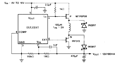
By using a MAX641 to drive separate P-and N-cbannel MOSFETs, both ends of the inductor are switched to allow non inverting buck/boost operation. A second advantage of the circuit over most boostonly designs is that the output goes to 0 V when shutdown is activated. Inefficiency is a drawback because two MOSFETs and two diodes increase the losses in the charge and discharge path of the inductor. The circuit delivers +12 V at 100 mA at 70 percent efficiency with an 8-V input.
Step up Down DC - DC Converter Circuit Diagram


No comments:
Post a Comment