Social Icons

Pages

Latch Debouncer Switch Circuit Diagram

This is a simple Latch De bouncer Switch Circuit Diagram In electronics latch is a circuit that has two stable states and can be used to store state information. Although this circuit uses a 74HC74, any CMOS variant of this flip-flop will work. IC1A acts as a true/ complement buffer. RI and R2 ensure that IC1A comes out of reset before the clock`s edge occurs. R3 applies IClA`s logic state to pins 1 and 3. When the switch closes, the next logic state stored on the capacitor transfers to the flip-flop`s reset and clock inputs.
Latch De bouncer Switch Circuit Diagram 


Releasing the switch lets the capacitor charge to the next state via R4. IClA`s output is the LSB; IClB`s output is the MSB. Notice that the counter`s state advances when the switch is first pressed, rather than when it`s released; the latter is the case with many other switch-debouncing schemes. You can replace RI with a 22-pF capacitor to reduce the circuit`s sensitivity to parasitic effects. The addition of this capacitor also lets you lower the magnitude of R2 and R3 by a factor of 10.

A Charge Pump Circuit Diagram

A charge pump is a kind of DC to DC converter that uses capacitors as energy storage elements to create either a higher or lower voltage power source.This is a Positive input and negative output charge pump. The 74Cl4 IC is a self-oscillating driver for the MOSFET power switch.


A Charge Pump Circuit Diagram


A Charge Pump Circuit Diagram


It produces a pulse width of 6.5 p,s at a repetition frequency of 100 kHz. When the MOSFET device is off, capacitor C is charged to the positive supply. When the power through the MOSFET switches on, C delivers a negative voltage through the series diode to the output. The zener serves as a dissipative regulator. Because the MOSFET switches fast, operation at high frequencies allows the capacitors in the system to be small.

Precision Full-Wave Ac-Dc Converter Circuit Diagram

A dc level is produced that corresponds to the ac input rms value (if sine wave), -i set the gain of IC2 to 1.11. This factor is the average-to-rms conversion factor. IC1 and IC2 act as a full-wave rectifier circuit, with Dl and D2. 

Precision Full-Wave Ac/Dc Converter Circuit Diagram


Precision Full-Wave Ac/Dc Converter Circuit Diagram

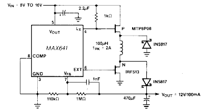
Step up Down DC - DC Converter Circuit Diagram

Positive output step-up and step-down dc-dc converters have a common limitation in that neither can handle input voltages that are both greater than or less than the output. For example, when converting a 12-V sealed lead/acid battery to a regulated +12 V output, the battery voltage might vary from a high of 15 V down to 10 V.


By using a MAX641 to drive separate P-and N-cbannel MOSFETs, both ends of the inductor are switched to allow non inverting buck/boost operation. A second advantage of the circuit over most boostonly designs is that the output goes to 0 V when shutdown is activated. Inefficiency is a drawback because two MOSFETs and two diodes increase the losses in the charge and discharge path of the inductor. The circuit delivers +12 V at 100 mA at 70 percent efficiency with an 8-V input.


Step up Down DC - DC Converter Circuit Diagram

Simple 12 -16V Converter Circuit Diagram

This is simple 12 -16V converter circuit diagram . Many devices operate from a car`s 12-V electrical system. Some require 12 V; others require some lesser voltage. An automobile battery`s output can vary from 12 to 13.8 V under normal circumstances. The load requirements of the device might vary.


This circuit maintains a constant voltage regardless of how those factors change. Simple circuit, A, uses a 7805 voltage regulator.In addition to a constant output, this JC provides overload and short-circuit protection. That unit is a 5-V, 1-A regulator, but when placed in circuit B, it can provide other voltages as well. When the arm of potentiometer R1 is moved toward ground, the output varies from 5 to about 10 V.


Simple 12 -16V Converter Circuit Diagram
 
Blogger Templates