The popular Timer IC 555 is extensively used in short duration timing applications. IC 555 is a highly stable integrated circuit functioning as an accurate time delay generator and free running multi vibrator. But one of the serious problem in 555 timer design is the false triggering of the circuit at power on or when voltage changes. The article describes how IC555 is designed perfectly to avoid false triggering.
555 IC pin functions
Pin1 Ground
Pin2 Trigger
Pin3 Output
Pin 4 Reset
Pin 5 Control voltage
Pin 6 Threshold
Pin 7 Discharge
Pin 8 Vcc
Functional aspects of pins
Trigger Pin 2
Usually pin2 of the IC is held high by a pull up resistor connected to Vcc. When a negative going pulse is applied to pin 2, the potential at pin 2 falls below 1/3 Vcc and the flip-flop switches on. This starts the timing cycle using the resistor and capacitor connected to pins 6 and 7.
Reset pin 4
Reset pin 4 can be controlled to reset the timing cycle. If pin 4 is grounded, IC will not be triggered. When pin4 becomes positive, IC becomes ready to start the timing cycle. Reset voltage is typically 0.7 volts and reset current 0.1 mA. In timer applications, reset pin should be connected to Vcc to get more than 0.7 volts.
Control Voltage pin 5
Pin5 can be used to control the working of IC by providing a DC voltage at pin5. This permits the control of the timing cycle manually or electronically. In monostable operation, the control pin5 is connected to ground through a 0.01 uF capacitor. This prevents the timing interval from being affected by AC or RF interference. In the Astable mode, by applying a variable DC voltage at pin 5 can change the output pulses to FM or PWM.
Threshold pin 6 and Discharge pin 7
These two inputs are used to connect the timing components- Resistor and Capacitor. The threshold comparator inside the IC is referenced at 2/3 Vcc and the trigger comparator is referenced at 1/3 Vcc. These two comparators control the internal Flip-Flop of the circuit to give High or Low output at pin 3.When a negative going pulse is applied to pin 2, the potential at pin2 drops below 1/3 Vcc and the trigger comparator switches on the Flip-Flop. This turns the output high. The timing comparator then charges through the timing resisto
and the voltage in the timing capacitor increases to 2/3 Vcc.( The time delay depends on the value of the resistor and capacitor.
That is, higher values, higher time).When the voltage level in the capacitor increases above 2/3 Vcc, the threshold comparator resets the Flip-Flop and the output turns low. Capacitor then discharges through pin 7.Once triggered, the IC will not responds to further triggering until the timing cycle is completed. The time delay period is calculated using the formula T= 1.1 Ct Rt. Where Ct is the value of Capacitor in PF and Rt is the value of Resistor in Ohms. Time is in Seconds.
How to eliminate false triggering?
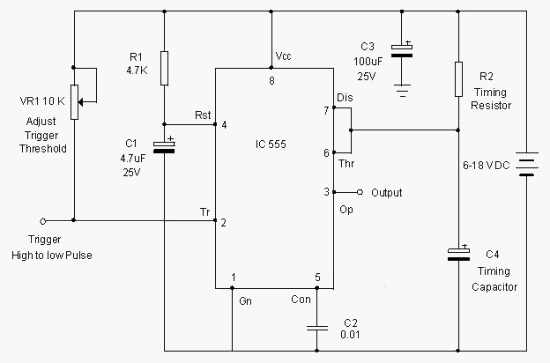
The circuit diagram shown below is the simple monostable using IC 555. To eliminate the false triggering resistor R1 and Capacitor C1 are connected to the reset pin 4 of the IC. So the reset pin is always high even if the supply voltage changes. Moreover capacitor C3 connected close to the Vcc pin 8 acts as a buffer to maintain stable supply voltage to pin 8. Using this design, it is easy to avoid false triggering to a certain extent.
555 Monostable circuit

A ready recknor to select timing resistor and capacitor

Theoretically long interval is possible with IC 555,but in practical conditions, it is difficult to get more than 3 minutes. If low leakage Tantalum capacitor is used, this can be increased to 5 minutes or more. If the value of the timing capacitor is too high above 470 uF, charging time will be prolonged which will upset the timing cycle and the output remains high even after the desired time is over.

No comments:
Post a Comment